Supercharge Your Innovation With Domain-Expert AI Agents!

Variable resistance memory device having an Anti-oxidation layer and a method of manufacturing the same

a memory device and variable resistance technology, applied in the field of memory devices, can solve problems such as the oxidation of a memory cell in the manufacturing of high-performance memory devices

Active Publication Date: 2020-04-16
SAMSUNG ELECTRONICS CO LTD
View PDF0 Cites 5 Cited by
  • Summary
  • Abstract
  • Description
  • Claims
  • Application Information

AI Technical Summary

Benefits of technology

This patent describes a variable resistance memory device and a method of manufacturing it. The device includes a plurality of lower electrodes, a plurality of variable resistors, a plurality of upper electrodes, and an interlayer insulating layer. An anti-oxidation layer is disposed between the plurality of variable resistors and the interlayer insulating layer to cover the side surfaces of the variable resistors. A capping layer is also disposed on top of the anti-oxidation layer to further protect it. The purpose of the anti-oxidation layer is to prevent oxidation of the material during manufacturing and use. The method includes the steps of forming the first conductive lines with an insulating pattern and stacking the layers to form the memory cells. The anti-oxidation layer is formed to protect the material, and the capping layer is added for further protection. The interlayer insulating layer is used to fill the space between the memory cells. Overall, this patent aims to improve the performance and reliability of variable resistance memory devices.

Problems solved by technology

However, oxidation of a memory cell in manufacturing of a high-performance memory device may occur.

Method used


Image

  • Variable resistance memory device having an Anti-oxidation layer and a method of manufacturing the same
  • Variable resistance memory device having an Anti-oxidation layer and a method of manufacturing the same
  • Variable resistance memory device having an Anti-oxidation layer and a method of manufacturing the same

Examples


Embodiment Construction

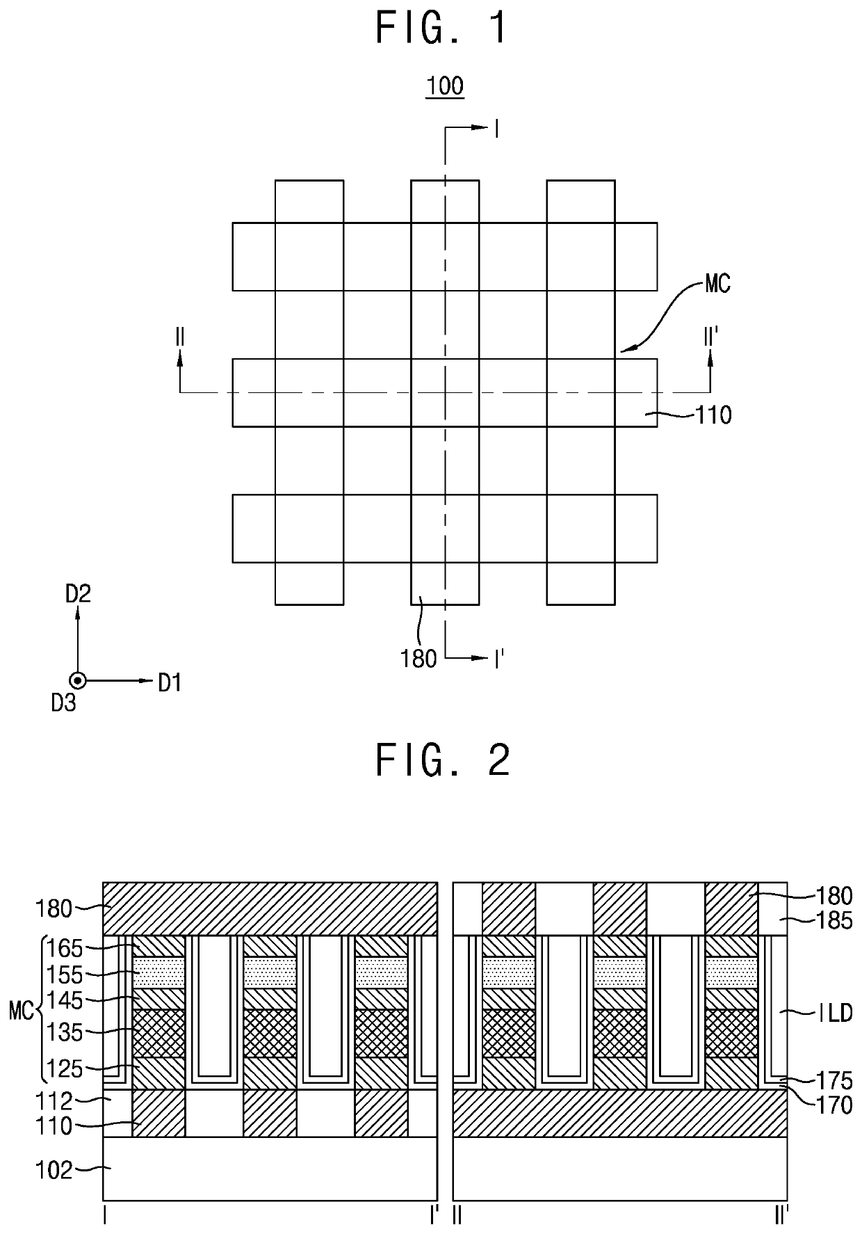
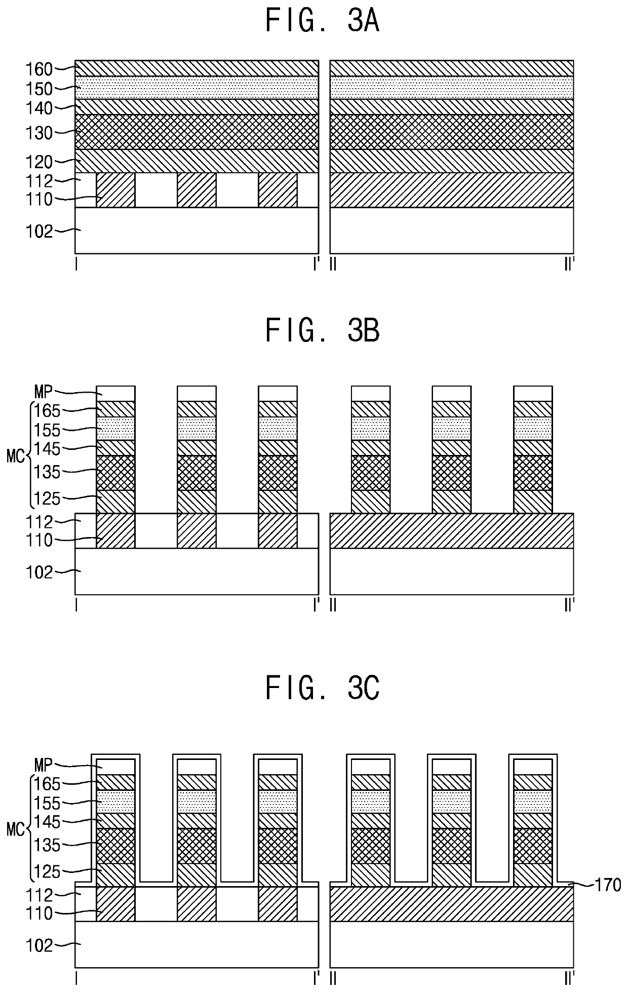
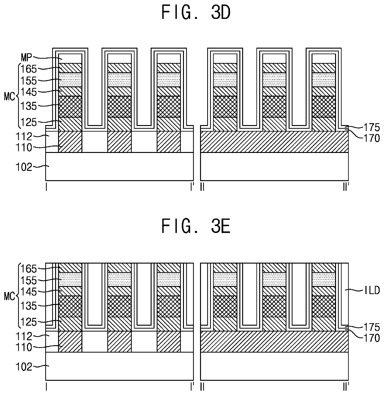
[0023]FIG. 1 is a plan view illustrating a memory cell array according to an exemplary embodiment of the present inventive concept. FIG. 2 shows cross-sectional views of a variable resistance memory device according to an exemplary embodiment of the present inventive concept. For example, FIG. 2 shows cross-sectional views of the variable resistance memory device taken along lines I-I′ and II-II′ of FIG. 1. For example, line I-I′ may extend in a second direction (e.g., a D2 direction) and the line II-II′ may extend in a first direction (e.g., a D1 direction) orthogonally intersecting the line represented by line I-I′.

[0024]Referring to FIGS. 1 and 2, a variable resistance memory device 100 according to the exemplary embodiment of the present inventive concept may include first conductive lines 110, second conductive lines 180, and memory cells MC. The first conductive line 110 may extend in a first direction (e.g., a D1 direction). The second conductive line 180 may extend in the se...


PUM


Abstract

A variable resistance memory device is provided including a plurality of lower electrodes disposed on a substrate. A plurality of variable resistors are disposed on the plurality of lower electrodes. A plurality of upper electrodes are disposed on the plurality of variable resistors. An interlayer insulating layer fills a space in the plurality of variable resistors. An anti-oxidation layer is disposed between the plurality of variable resistors and the interlayer insulating layer. The anti-oxidation layer covers side surfaces of the plurality of variable resistors, and the anti-oxidation layer comprises silicon and / or carbon.

Description

CROSS-REFERENCE TO RELATED APPLICATIONS[0001]This U.S. non-provisional patent application claims priority under 35 U.S.C. § 119 to U.S. Provisional Patent Application No. 62 / 746,220, filed on Oct. 16, 2018 and Korean Patent Applications No. 10-2019-0037630, filed on Apr. 1, 2019, and Korean Patent Application No. 10-2019-0060777, filed on May 23, 2019, the disclosures of which are incorporated by reference herein in their entireties.TECHNICAL FIELD[0002]The present disclosure provided herein relates to a memory device, and more particularly, to a variable resistance memory device including an anti-oxidation layer and a method of manufacturing the same.DISCUSSION OF RELATED ART[0003]As a semiconductor device becomes highly integrated, a memory having high performance, such as fast operation and a low operating voltage, is required. Recently, as novel memory devices, memory devices having variable resistance characteristics are being developed. For example, as variable resistance memo...

Claims


Application Information

Patent Timeline
IPC IPC(8): H01L43/08H01L27/22H01L27/24H01L45/00H01L43/10H01L43/12
CPCH01L43/08H01L45/1691H01L45/1675H01L43/12H01L45/141H01L27/2463H01L43/10H01L27/222H01L45/1253H10B61/20H10B63/24H10B63/80H10N70/882H10N50/01H10N70/063H10B61/00H10N50/10H10N50/85H10N70/068H10N70/841
Inventor AHN, SANGHOONKWON, OIKPARK, JEONGHEEHWANG, KIHYUN
Owner SAMSUNG ELECTRONICS CO LTD
Features
  • R&D
  • Intellectual Property
  • Life Sciences
  • Materials
  • Tech Scout
  • Unparalleled Data Quality
  • Higher Quality Content
  • 60% Fewer Hallucinations
Learn More