Phase-change memory device and manufacturing method thereof

a technology of phase-change memory and manufacturing method, which is applied in the direction of digital storage, semiconductor devices, instruments, etc., can solve the problems of increasing the number of processing steps, complicated whole manufacturing process of the device, and the inability to use above-mentioned conventional technology for mass production, etc., and achieves the effect of reducing process cost, high yield and easy manufacturing

Inactive Publication Date: 2005-01-27
LEE HEON
View PDF14 Cites 218 Cited by
  • Summary
  • Abstract
  • Description
  • Claims
  • Application Information

AI Technical Summary

Benefits of technology

[0019] Accordingly, the present invention has been made keeping in mind the above problems occurring in the prior art, and an object of the present invention is to provide a phase change memory device having a new structure which can be easily manufactured by mass-production with a high yield rate, therefore, reducing the cost of process and providing reliable device characteristics, and a manufacturing method thereof.

Problems solved by technology

Therefore, total number of processing steps should be increased and the whole manufacturing process of the device becomes complicated.
On the other hand, the above mentioned conventional technology can not be used for mass production because the holes 145 are too much narrowed by the sidewalls 142 and therefore it is very difficult to fill the holes 145 without voids using conventional metallic materials.
However, additional steps, such as depositing the first dielectric film, depositing the sacrificial layer, etching the sacrificial layer and etching the first dielectric film, are required so that the process is more complicate.
Therefore, high productivity in manufacturing cannot be expected.
In addition, the problem related to the voids formation in contact filling process as mentioned above still remains.
However, it is extremely difficult to control wet etch process precisely.
Therefore, it is very difficult to obtain process margin and uniform tip structure reproducibly for mass production.
Such disparities may cause problems related to the reproducibility and reliability of the devices' characteristics, therefore limiting application of the conventional technology for mass production of the phase-change memory devices.

Method used


Image

  • Phase-change memory device and manufacturing method thereof
  • Phase-change memory device and manufacturing method thereof
  • Phase-change memory device and manufacturing method thereof

Examples


Embodiment Construction

[0060] Reference now should be made to the drawings, in which the same reference numerals are used throughout the different drawings to designate the same or similar components.

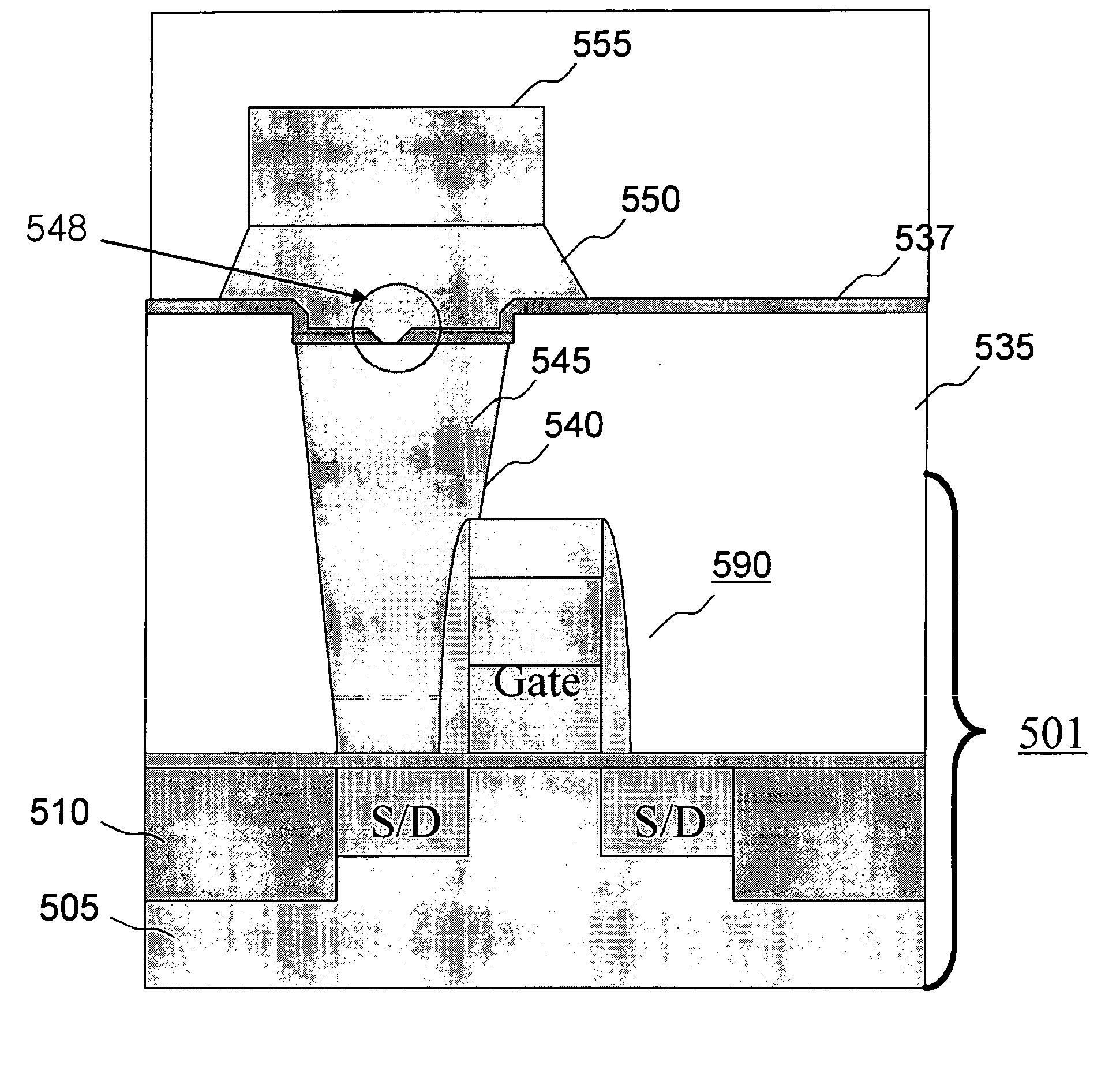
[0061] In FIG. 6, a phase-change memory device structure according to a preferred embodiment of the present invention is exemplified. An FET 590 is formed below a phase-change resistor 550 through a conventional CMOS process technology. In the structure, 1 memory cell includes 1 FET and 1 phase-change resistor. The structure below the phase-change resistor 550 can be variously modified in accordance with the specification which is required to meet in each of the detailed applications. For an example of the modifications, a LOCOS (Local Oxidation of Silicon) structure can replace the STI (Shallow Trench Isolation) structure 510 shown in FIG. 6 as a device isolation structure. For another example of the modifications, another type of switching device such as a BJT (Bipolar Junction Transistor) can replaced the...


PUM


Abstract

The present invention is to provide a phase change memory device having a new structure which can be easily manufactured by mass-production with a high yield rate, therefore, reducing the cost of process and providing reliable device characteristics, and a manufacturing method thereof. The present invention provides a phase-change memory device comprising: a lower dielectric layer; a lower electrode, at least a part of the lateral surface of the lower electrode being surrounded by the lower dielectric layer; a thin dielectric layer including a pore having smaller area than the top surface of the lower electrode, aligned to the top surface of the lower electrode and extending to the top surface of the lower electrode; and a phase-change resistor filling the pore and formed on the thin dielectric layer. In the proposed structure of the present invention, the pores or local damaged spots can provide a micro path of current and localize the phase-changing volume in the phase-change resistor. Thus, the phase-change memory device can be operated with very low power.

Description

BACKGROUND OF THE INVENTION [0001] 1. Field of the Invention [0002] The present invention relates generally to a phase-change memory device and a manufacturing method thereof, and, more particularly, to a phase-change memory device having a new structure which can be easily manufactured by mass-production with a high yield rate, therefore, reducing the cost of process and providing reliable device characteristics. [0003] 2. Description of the Related Art [0004] With expansion of mobile devices the demand for non-volatile memory devices are growing rapidly. Among the non-volatile memory devices which are widely used, the flash memory, the ferro-electric memory, the magnetic memory and the phase-change memory are leading the next generation of the non-volatile memory devices. Especially, the phase-change memory is being widely studied as it can resolve the flash memory's disadvantages including slow access speed, limited number of use times (about 105˜106 times) and high voltage requi...

Claims


Application Information

Patent Timeline
Patent Type & Authority Applications(United States)
IPC IPC(8): H01L27/24H01L45/00
CPCH01L45/06H01L45/1233H01L45/1246H01L27/2463H01L45/16H01L27/2409H01L27/2436H01L45/144H10B63/20H10B63/30H10B63/80H10N70/231H10N70/828H10N70/826H10N70/8828H10N70/011
Inventor LEE, HEON
Owner LEE HEON
Why Eureka
Try Eureka