Electroluminescent display devices

a display device and electroluminescent technology, applied in the field of electroluminescent display devices, can solve the problems of difficult data correction techniques, affecting the brightness of the display, and not being able to place this preferred cathode material against the active matrix circuitry,

Inactive Publication Date: 2009-06-30
INNOLUX CORP
View PDF11 Cites 221 Cited by
  • Summary
  • Abstract
  • Description
  • Claims
  • Application Information

AI Technical Summary

Benefits of technology

[0043]This method again uses feedback to produce a desired current through the display element, but allows tolerance differences in the resistance value.

Problems solved by technology

One problem with voltage-programmed pixels, particularly using polysilicon thin film transistors, is that different transistor characteristics across the substrate (particularly the threshold voltage) give rise to different relationships between the gate voltage and the source-drain current, and artefacts in the displayed image result.
A further problem with LED displays arises from the significant currents drawn by the pixels.
This is the preferred arrangement because the desired cathode material of the EL display element is opaque, so that the emission is from the anode side of the EL diode, and furthermore it is not desirable to place this preferred cathode material against the active matrix circuitry.
The significant row conductor resistance gives rise to voltage drops along the row conductors, and these voltage variations along the power supply line alter the gate-source voltage on the drive transistors, and thereby affect the brightness of the display.
Furthermore, as the currents drawn by the pixels in the row are image-dependent, it is difficult to correct the pixel drive levels by data correction techniques, and the distortion is essentially a cross talk between pixels in different columns.
Nevertheless significant voltage drops are still present.
These voltage drops also give rise to performance limitations in current mirror pixel circuits, and thin film transistors are inherently non-ideal current source devices (the output current will in fact depend on both the source and drain voltages rather than only on the gate-source voltage).

Method used


Image

  • Electroluminescent display devices
  • Electroluminescent display devices
  • Electroluminescent display devices

Examples


Embodiment Construction

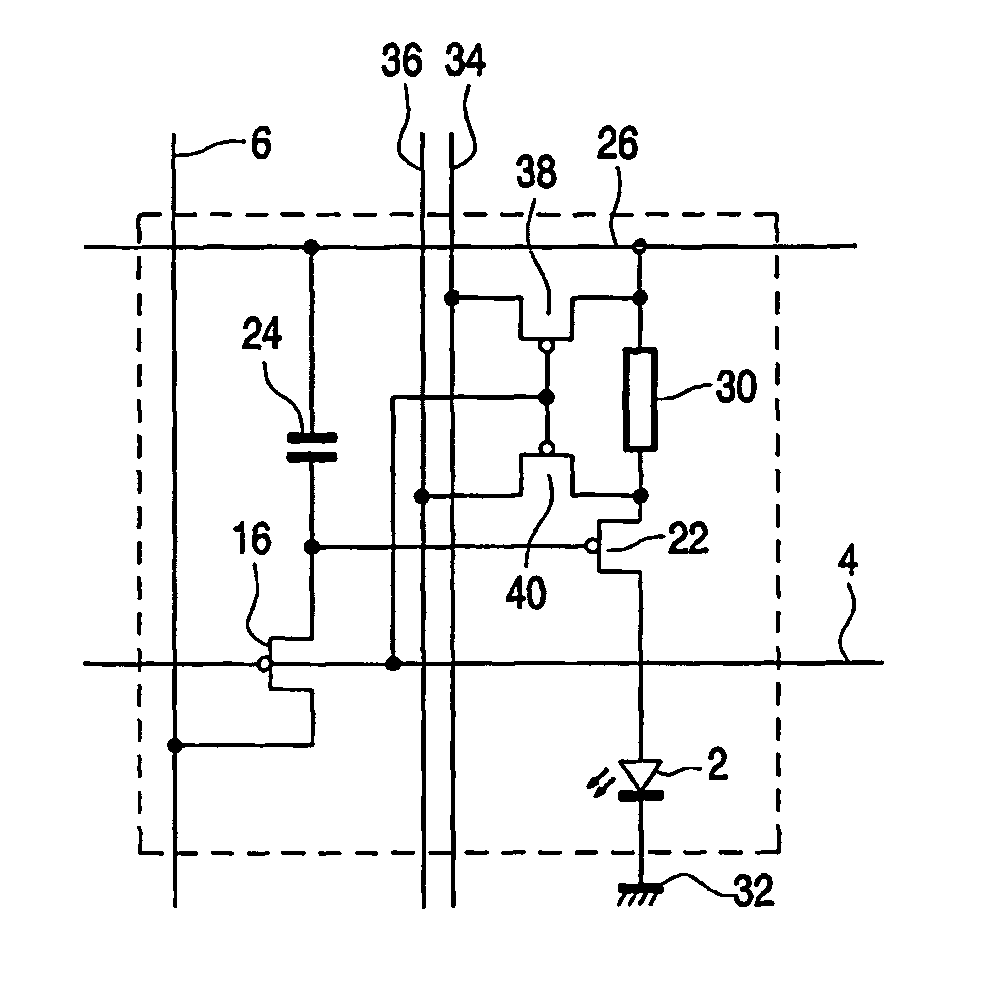
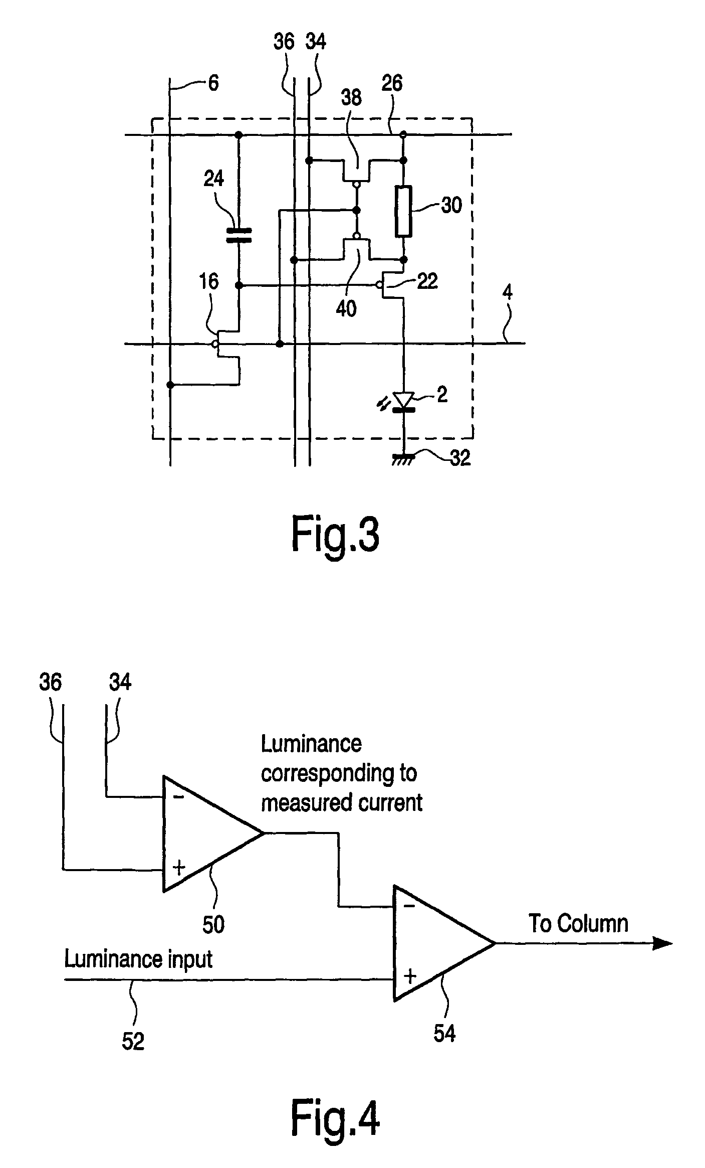
[0052]The invention provides an active matrix electroluminescent display device in which a current sampling resistor is provided within each pixel in the main current path of the display element. This enables a feedback signal derived from the current through the resistor (and therefore the display element) to be used to control the pixel drive.

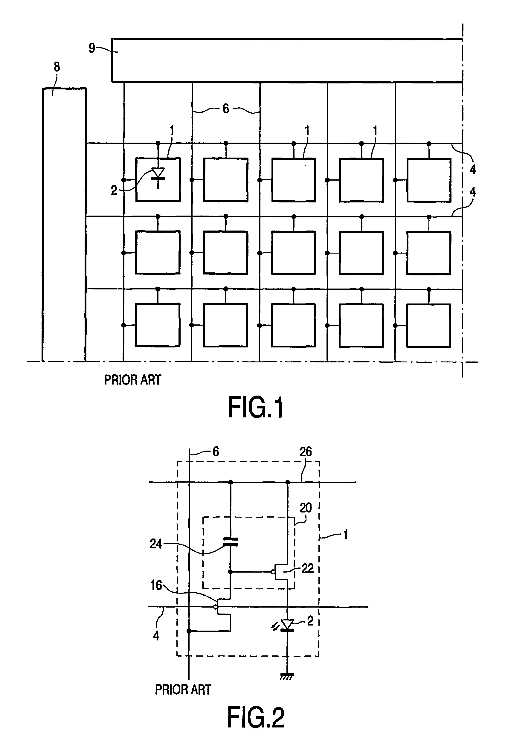
[0053]The same reference numerals are used in different figures for the same components, and description of these components will not be repeated.

[0054]FIG. 3 shows a first pixel arrangement in accordance with the invention. As in the conventional pixel of FIG. 2, the pixel is voltage-addressed, and a storage capacitor 24 holds the voltage on the gate of the drive transistor 22 after the pixel addressing phase.

[0055]A current sampling resistor 30 is placed in series with the drive transistor 22 and the display element 2, so that they are all arranged in series between the power supply line 26 and the ground terminal 32. The voltage at each en...


PUM


Abstract

An active matrix electroluminescent display device has a current sampling resistor within each pixel in series with the display element. A feedback signal represents the voltage drop across the current sampling resistor and the pixel drive signals are modified in dependence on the feedback signal to control the current driven through the display element. In this way, threshold compensation is provided, whilst enabling a single voltage-driven drive transistor to be employed.

Description

BACKGROUND OF THE INVENTION[0001](1) Field of the Invention[0002]This invention relates to electroluminescent display devices, particularly active matrix display devices having thin film switching transistors associated with each pixel.[0003](2) Description of Related Art[0004]Matrix display devices employing electroluminescent, light-emitting, display elements are well known. The display elements may comprise organic thin film electroluminescent elements, for example using polymer materials, or else light emitting diodes (LEDs) using traditional III-V semiconductor compounds. Recent developments in organic electroluminescent materials, particularly polymer materials, have demonstrated their ability to be used practically for video display devices. These materials typically comprise one or more layers of a semiconducting conjugated polymer sandwiched between a pair of electrodes, one of which is transparent and the other of which is of a material suitable for injecting holes or elec...

Claims


Application Information

Patent Timeline
Patent Type & Authority Patents(United States)
IPC IPC(8): G06F15/16G09G3/30G09G3/32
CPCG09G3/3233G09G2300/0809G09G2320/043G09G2320/0295G09G2300/0842G09G3/30G09G3/32G09G3/20
Inventor STEER, WILLIAM A.
Owner INNOLUX CORP
Why Eureka
Try Eureka