Method for manufacturing printed circuit board, printed circuit board and drive circuit board

a manufacturing method and printed circuit board technology, applied in the field of electronic circuits, can solve the problems of no application universality of related electronic devices, and high manufacturing cost of printed circuit boards. , to achieve the effect of ensuring physical safety of pads, low manufacturing cost and simplifying the manufacturing steps of printed circuit boards

Inactive Publication Date: 2020-04-16
CHONGQING HKC OPTOELECTRONICS TECH CO LTD +1
View PDF8 Cites 0 Cited by
  • Summary
  • Abstract
  • Description
  • Claims
  • Application Information

AI Technical Summary

Benefits of technology

[0041]In the above method for manufacturing the printed circuit board, each of the pad on the printed circuit board includes a pad body and a protrusion extending from a side of the pad body, and adjacent two of the pads are correspondingly arranged by the protrusion, and there is a short spatial distance between the protrusions of different pads, therefore the different pads are closer to each other through the protrusion. Through providing an electrical isolation region between the protrusions of adjacent two of the pads, overlapping a steel screen on the surface of the printed circuit board, and meshes are provided on the steel screen, and the meshes respectively corresponds to at least part of two pads and the electrical isolation region between the two pads. Since tin paste has fluidity, the solder paste will pass through the meshes of the steel screen and flows onto the electrical isolation region on the printed circuit board, and the protrusions of the different pads are electrically connected by the tin paste. Meanwhile, the tin paste cannot pass through the region without meshes in the steel screen, thus ensuring physical safety of the pads within the printed circuit board. Therefore, the method for manufacturing the printed circuit board in the present application can achieve electrical connection between the two pads by adding the tin paste between the protrusions of the pads, there is no requirement for an additional 0Ω resistor, and the manufacturing cost is low. Moreover, no special punching operation is required on the printed circuit board, which simplifies the manufacturing steps of the printed circuit board and is easy to implement, and greatly improves application range of the method for manufacturing the printed circuit board, and has high practicability. Therefore, the present application effectively solves the problems, in the exemplary technology, that the method for manufacturing the printed circuit board must use a 0Ω resistor to implement electrical connection, thus resulting in high manufacturing cost of the printed circuit board, complicated manufacturing process, and difficulty in universal application.

Problems solved by technology

The present application provides a manufacturing method for a printed circuit board, a printed circuit board and a drive circuit board, which aims at solving the problem, in the conventional technologies, that the method for manufacturing the printed circuit board has to use a 0Ω resistor to establish the electrical connection, thus leading to relatively high manufacturing cost for the printed circuit board, much cumbersome manufacturing process, and no application universality of related electronic device.

Method used


Image

  • Method for manufacturing printed circuit board, printed circuit board and drive circuit board
  • Method for manufacturing printed circuit board, printed circuit board and drive circuit board
  • Method for manufacturing printed circuit board, printed circuit board and drive circuit board

Examples


Embodiment Construction

[0050]In order to make the purpose, technical solutions and advantages of the present application more clear, the present application will be further described in detail below with reference to the drawings and embodiments. It should be understood that, the specific embodiments described herein are merely for explaining the present application, and not intended to limit the present application.

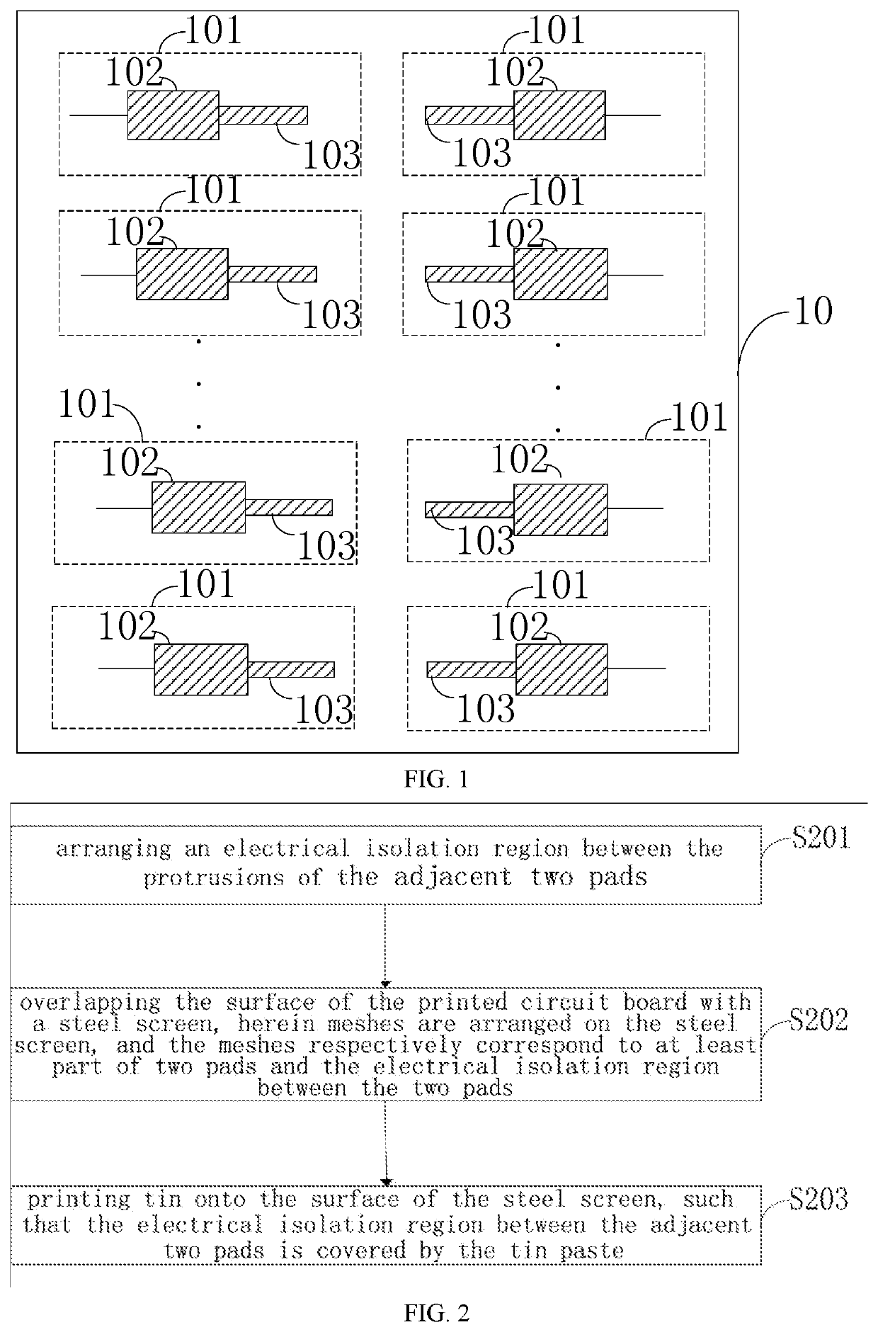
[0051]It should be noted that, in the printed circuit board, the connection method between different pads is a key factor affecting the manufacturing cost of the printed circuit board and the circuit functions of the printed circuit board. Moreover, with the rapid development of the manufacturing process of the printed circuit board, in an exemplary technology, the conventional printed circuit board uses a 0Ω resistor to establish electrical connection between adjacent pads, given the relatively long distance between the adjacent pads. Herein, The 0Ω resistor acts as a jumper resistor, and is ...


PUM


Abstract

The present application pertains to the technical field of electronic circuits, and provides a method for manufacturing a printed circuit board, herein a side of each of the pads within the printed circuit board extends outward to form a protrusion, and an electrical isolation region between the protrusions of adjacent two pads is covered with tin paste.

Description

CROSS-REFERENCE TO RELATED APPLICATIONS[0001]This application is the International Application No. PCT / CN2018 / 110496 for entry into US national phase with an international filing date of Oct. 16, 2018, designating US, now pending, and claims priority to Chinese Patent Application No. 201810979524.8, filed on Aug. 27, 2018, the content of which is incorporated herein by reference in its entirety.BACKGROUND OF THE INVENTIONField of the Invention[0002]The present application pertains to the technical field of electronic circuits, and particularly to a manufacturing method for a printed circuit board, a printed circuit board and a drive circuit board.Description of Related Art[0003]In a conventional electronic device, a printed circuit board is a core component of the electronic device. Since the printed circuit board is provided with various power supply circuits, various functional functions can be realized through the functional circuits, thus the printed circuit board is responsible...

Claims


Application Information

Patent Timeline
Patent Type & Authority Applications(United States)
IPC IPC(8): H05K1/11H05K1/02H05K3/24G09G3/22
CPCH05K1/111H05K1/0287G09G3/22H05K3/24G09G3/36H05K1/116H05K2201/09381H05K2201/09427H05K2201/2036G06F3/147H05K3/1233H05K2203/173
Inventor ZHAO, WENQIN
Owner CHONGQING HKC OPTOELECTRONICS TECH CO LTD
Why Eureka
Try Eureka