Contact Etchback in Room Temperature Ionic Liquid

a technology of ionic liquid and contact etchback, which is applied in the direction of semiconductor/solid-state device manufacturing, basic electric elements, electric apparatus, etc., can solve the problems of increasing complexity in design and manufacturing of devices incorporating, scaling down,

Active Publication Date: 2020-04-30
TAIWAN SEMICON MFG CO LTD
View PDF0 Cites 0 Cited by
  • Summary
  • Abstract
  • Description
  • Claims
  • Application Information

AI Technical Summary

Problems solved by technology

However, such scaling down has also been accompanied by increased c...

Method used


Image

  • Contact Etchback in Room Temperature Ionic Liquid
  • Contact Etchback in Room Temperature Ionic Liquid
  • Contact Etchback in Room Temperature Ionic Liquid

Examples


Embodiment Construction

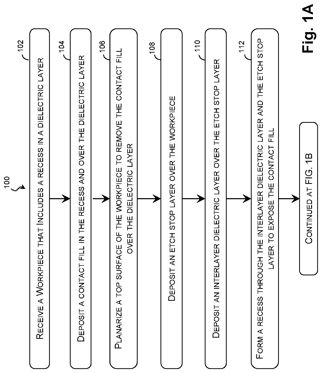
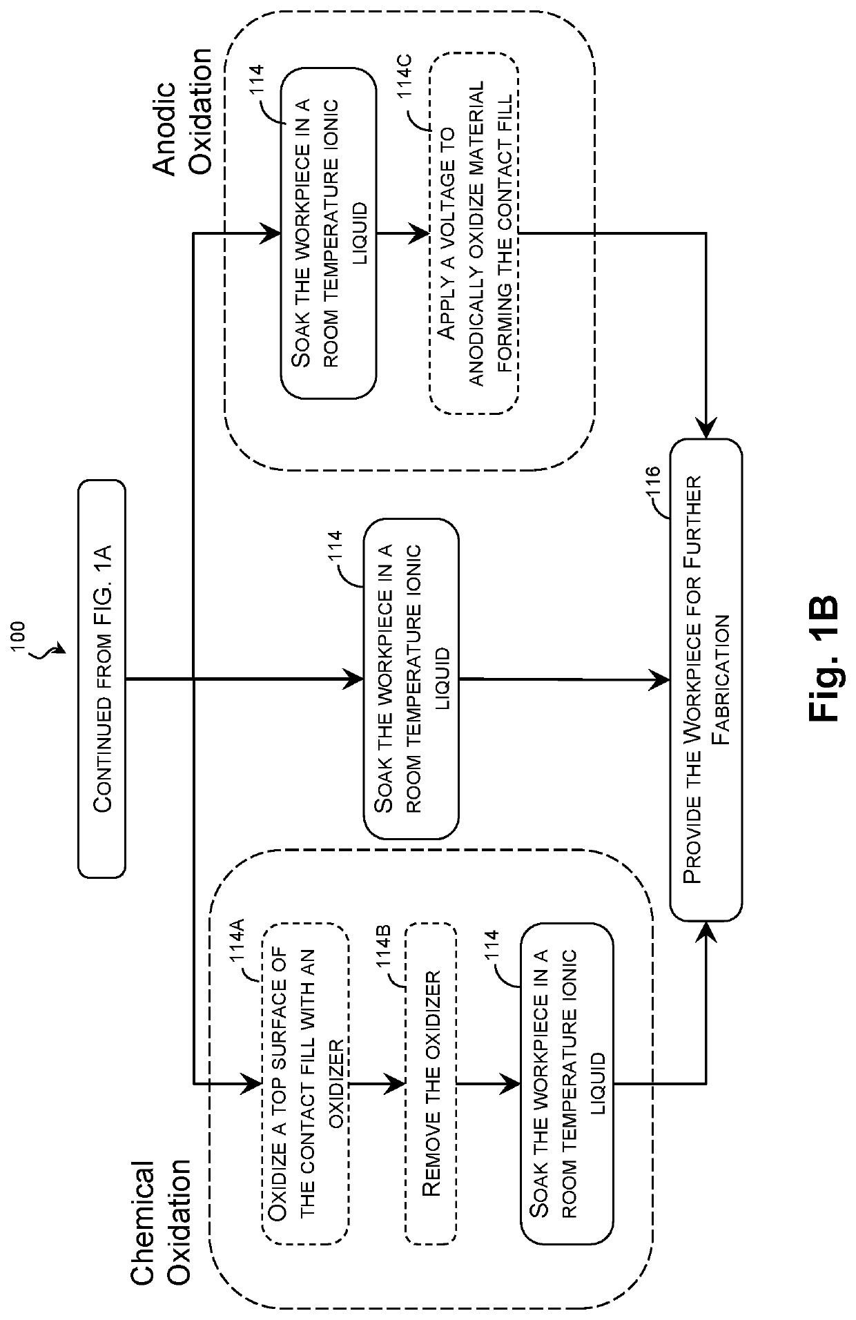
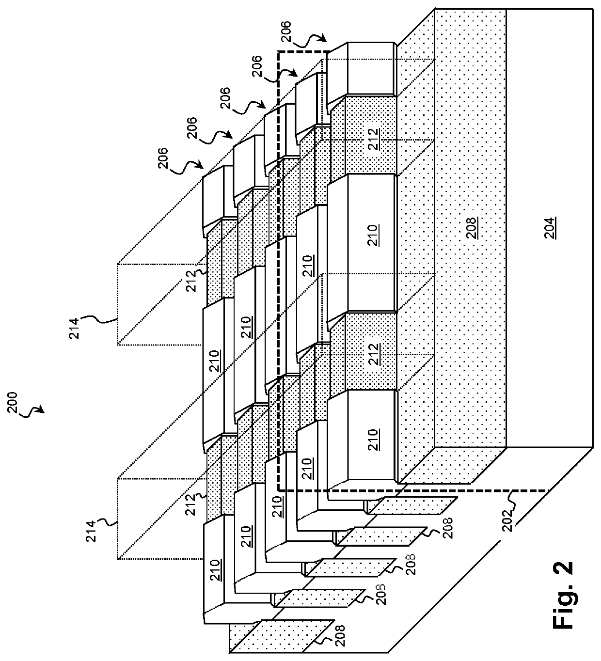
[0008]The following disclosure provides many different embodiments, or examples, for implementing different features of the disclosure. Specific examples of components and arrangements are described below to simplify the present disclosure. These are, of course, merely examples and are not intended to be limiting. For example, the formation of a first feature over or on a second feature in the description that follows may include embodiments in which the first and second features are formed in direct contact, and may also include embodiments in which additional features may be formed between the first and second features, such that the first and second features may not be in direct contact. Moreover, the formation of a feature connected to and / or coupled to another feature in the present disclosure that follows may include embodiments in which the features are formed in direct contact, and may also include embodiments in which additional features may be formed interposing the featur...


PUM

PropertyMeasurementUnit
Electric potential / voltageaaaaaaaaaa
Temperatureaaaaaaaaaa

Abstract

The present disclosure provides an integrated circuit with an interconnect structure and a method for forming the integrated circuit. In one embodiment, a method of the present disclosure includes receiving a workpiece that includes a first recess in a dielectric layer over the workpiece, depositing a contact fill in the first recess and over the dielectric layer to form a contact feature, planarizing a top surface of the workpiece to remove the contact fill over the dielectric layer, depositing an interlayer dielectric layer over the planarized top surface of the workpiece, forming a second recess in the interlayer dielectric layer to expose the contact fill in the dielectric layer, recessing the contact fill by soaking the workpiece in a room temperature ionic liquid, and depositing a conductive layer over the recessed contact fill. The material forming the contact fill is soluble in the room temperature ionic liquid.

Description

PRIORITY DATA[0001]The present application claims the benefit of U.S. Provisional Application No. 62 / 752,554, entitled “Method for Ruthenium Etch Without Ruthenium Oxide Formation in a Toom-Temperature Ionic Liquid,” filed Oct. 30, 2018, herein incorporated by reference in its entirety.BACKGROUND[0002]The semiconductor integrated circuit (IC) industry has experienced rapid growth. In the course of IC evolution, functional density (i.e., the number of interconnected devices per chip area) has generally increased while geometry size (i.e., the smallest component (or line) that can be created using a fabrication process) has decreased. This scaling down process generally provides benefits by increasing production efficiency and lowering associated costs. However, such scaling down has also been accompanied by increased complexity in design and manufacturing of devices incorporating these ICs. Parallel advances in manufacturing have allowed increasingly complex designs to be fabricated ...

Claims


Application Information

Patent Timeline
IPC IPC(8): H01L21/768H01L21/285
CPCH01L21/76883H01L21/7684C23F1/10H01L21/76802H01L21/28556H01L21/76838H01L21/76877H01L21/823431H01L21/823475H01L21/28518H01L21/32134H01L21/76804H01L21/76805H01L21/76814H01L21/76831H01L21/76843H01L21/76855H01L21/76856H01L21/76897
Inventor KELLY, ANDREW JOSEPH
Owner TAIWAN SEMICON MFG CO LTD
Why Eureka
Try Eureka