Communication device and electronic device having protective function

a communication device and electronic device technology, applied in the direction of exchanging data chargers, safety/protection circuits, transportation and packaging, etc., can solve the problems of communication circuit damage, nfc module damage, communication circuit damage, etc., to prevent the damage of an inductive type communication device and not supply excessive energy

Inactive Publication Date: 2020-08-27
MAPS
View PDF0 Cites 3 Cited by
  • Summary
  • Abstract
  • Description
  • Claims
  • Application Information

AI Technical Summary

Benefits of technology

[0018]In one embodiment, a communication device can be protected when wireless charging is performed. In particular, a communication circuit of a communication device using an antenna or an inductive device, such as a near-field communication (NFC) device or a magnetic secure transmission (MST) device, can be protected so as to not supply excessive energy thereto due to a field applied from the outside. The communication device is protected by blocking the supply of a power signal thereto during the wireless charging. Accordingly, it is possible to prevent an inductive type communication device from being damaged due to the supply of excessive power thereto when the power signal is supplied from a power transmitting unit.
[0019]The present invention is applicable to protecting the communication device from a wireless charging sys

Problems solved by technology

In general, low power is transmitted from or received by the NFC module and thus excessive power is supplied to the NFC module and the NFC module may be damaged when a large amount of power is supplied thereto from th

Method used


Image

  • Communication device and electronic device having protective function
  • Communication device and electronic device having protective function
  • Communication device and electronic device having protective function

Examples


first embodiment

[0061]FIG. 6 is a circuit diagram of a communication device which protects a communication circuit according to the present invention.

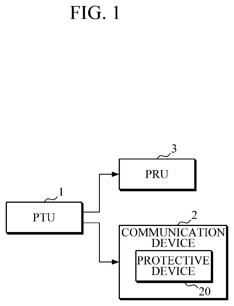
[0062]Referring to FIG. 6, a communication device 2 includes a resonator 22, a communication circuit 24, and a protective device 20. The protective device 20 may include a wireless power input detector 200 and may further include a protective circuit 202.

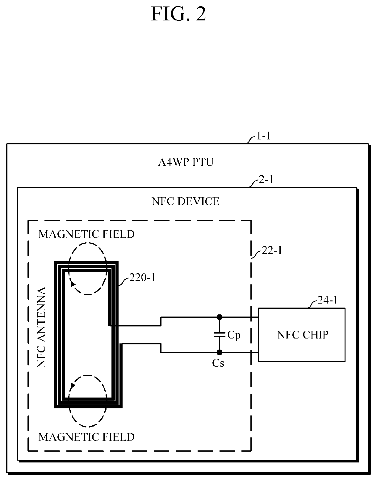
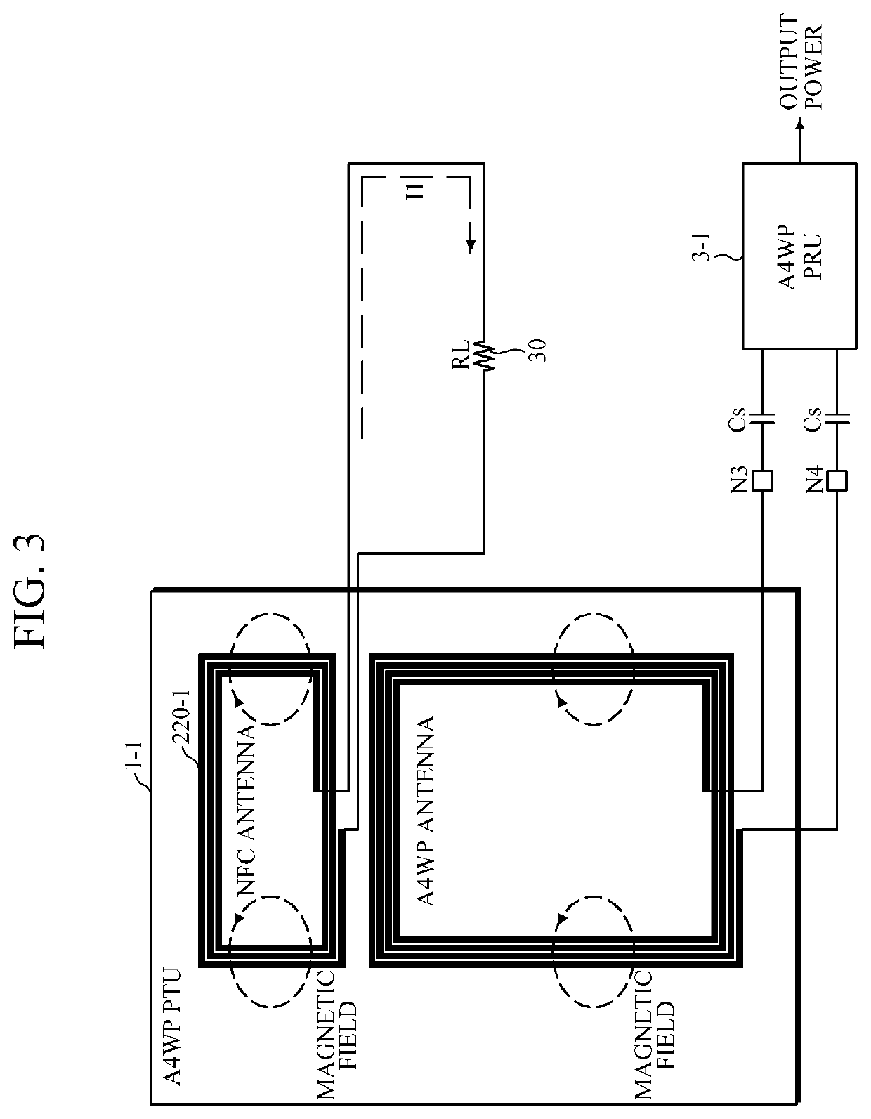
[0063]The resonator 22 includes an antenna 220 and a capacitor Cs 222. The antenna 220 includes an inductance component. An inductive device may be provided instead of the antenna 220. A transceiving device such as the antenna 220 or the inductive device generates a magnetic field or transmits or receives a signal in response to a magnetic field. When the communication device 2 is an NFC device, the antenna 220 may be an NFC antenna.

[0064]The communication circuit 24 is selectively connected to the antenna 220. If the communication circuit 24 and the antenna 220 are connected to each other, the commun...

second embodiment

[0073]FIG. 7 is a circuit diagram of a communication device which protects a communication circuit according to the present invention.

[0074]The communication device of FIG. 7 further includes impedance devices Z1204-1 and Z2204-2, as compared to the communication device 2 of FIG. 6. If a communication circuit 24 is protected using switching devices M1202-1 and M2202-2, excessive current may be supplied to the switching devices M1202-1 and M2202-2 via an antenna 220 when turn-on resistances of the switching devices M1202-1 and M2202-2 are low. Thus, as illustrated in FIG. 7, the impedance devices Z1204-1 and Z2204-2 are provided between the antenna 220 and the communication circuit 24 to change a resonance frequency of a resonator 22 and prevent excessive current from flowing to the switching devices MI 202-1 and M2202-2. In this case, the amount of received current may be reduced by reducing the resonance frequency of the resonator 22 to be lower than a frequency input to the antenn...

third embodiment

[0077]FIG. 8 is a circuit diagram of a communication device which protects a communication circuit according to the present invention.

[0078]The communication device of FIG. 8 further includes a frequency sensor 206, as compared to the communication device of FIG. 7. In some cases, a communication circuit 24 may be protected by determining whether a specific frequency is input by using the frequency sensor 206 which senses a frequency from an input signal of a rectifier 240 of the communication circuit 24.

[0079]In detail, the protective device 20 includes a wireless power input detector 200, a protective circuit 202, impedance devices 204-1 and 204-2, the frequency sensor 206, and a logic circuit 208. The wireless power input detector 200 detects a wireless power signal and generates a control signal for protecting the communication circuit 24. The frequency sensor 206 senses a frequency of a rectifier input signal input to the rectifier 240 of the communication circuit 24 and determ...


PUM


Abstract

Provided are a communication device and an electronic device each having a protective function. In one embodiment, the communication device includes a transceiving device configured to transmit or receive a signal, a communication circuit configured to be selectively connected to the transceiving device, and a wireless power input detector configured to protect the communication circuit from a wireless power signal by detecting whether the signal is the wireless power signal which is input for charging and generating a control signal for selectively disconnecting the communication circuit from the transceiving device.

Description

TECHNICAL FIELD[0001]The present invention relates to wireless power transmitting and receiving technology.BACKGROUND ART[0002]A short-range communication module establishing communication by forming a magnetic field of a frequency band of several to several tens of MHz has been applied and used as a module for radio-frequency identification (hereinafter referred to as ‘RFID’), near-field communication (hereinafter referred to as ‘NFC’), etc. Especially, various applications using an NFC method have been applied to portable terminals such as cellular phones and have attracted much attention as auxiliary payment means.[0003]Wireless charging is performed at a low frequency band of 100 kHz in the Qi of the Wireless Power Consortium (hereinafter referred to as ‘WPC’) or a Power Matters Alliance (PMA) method, which is an inductive type wirelessly charging methods. In contrast, NFC is established using an Industry-Science-Medical band of 13.56 MHz (hereinafter referred to as the ‘ISM ban...

Claims


Application Information

Patent Timeline
IPC IPC(8): H02J50/12H02J50/70H02J7/04
CPCH02J50/70H02J50/12H02J7/04H02J7/0029H02J7/02H04B5/0037H04B5/0075H02J7/00034H02J13/00022
Inventor RHEE, JOONHWANG, JONG TAESHIN, HYUN ICKJIN, KI WOONG
Owner MAPS
Why Eureka
Try Eureka