Unlock instant, AI-driven research and patent intelligence for your innovation.

Pixel compensating circuit and pixel compensating method

a pixel compensating circuit and pixel compensating technology, applied in the field of display technology, can solve the problems of irregular voltage, affecting the display quality of the oled panel, unstable driving current of the organic light-emitting diode oled, etc., to improve the uniformity improve the aging phenomenon of the driving transistor, and improve the effect of the driving transistor

Active Publication Date: 2020-10-15
WUHAN CHINA STAR OPTOELECTRONICS SEMICON DISPLAY TECH CO LTD
View PDF0 Cites 1 Cited by
  • Summary
  • Abstract
  • Description
  • Claims
  • Application Information

AI Technical Summary

Benefits of technology

This patent is about a new pixel compensating circuit and method that can help improve the performance and consistency of a driving transistor in a display. The technical effect of this patent is to reduce the aging of the transistor and make it more uniform in its performance.

Problems solved by technology

Because the threshold voltage of the thin film transistor T2 easily drifts, which makes a driving current of the organic light-emitting diode OLED unstable and affects display quality of the OLED panel.
However, the above-mentioned 7T1C pixel compensating circuit still has problems of irregular voltages between threshold voltage and the discharging region.
Therefore, electrical current may leak when a display grayscale of pixels is at low level which causes unlikeness of a displayed grayscale to a desired grayscale and causes poor contrast of the display panel.

Method used


Image

  • Pixel compensating circuit and pixel compensating method
  • Pixel compensating circuit and pixel compensating method
  • Pixel compensating circuit and pixel compensating method

Examples


Embodiment Construction

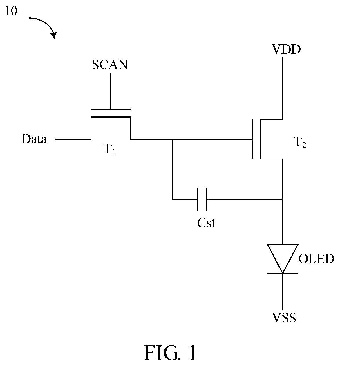
[0030]The display panel and the display device provided by the present disclosure will be described in detail below with reference to the accompanying drawings. The longitudinal, lateral, upper, lower, left, right, front, and rear aspects of the detailed description are merely for convenience of describing the relative relationship between the components rather than limitations of embodiments of the present disclosure. It is apparent that the described embodiments only exemplify a part of the embodiments of the disclosure. All other embodiments which can be obtained by a person of ordinary skill in the art based on the embodiments of the present disclosure without creative efforts fall within the scope of the present disclosure.

[0031]The display panel and the display device provided by the present disclosure will be described in detail below with reference to the accompanying drawings. The longitudinal, lateral, upper, lower, left, right, front, and rear aspects of the detailed desc...


PUM

PropertyMeasurementUnit
voltageaaaaaaaaaa
voltage potentialaaaaaaaaaa
threshold voltageaaaaaaaaaa

Abstract

A pixel compensating circuit comprises an organic light-emitting diode (OLED), a first transistor, a compensating transistor, a storage capacitor, a second transistor, a third transistor, and a seventh transistor. If a present-stage scan signal is at a low voltage potential, the second transistor is turned on, the gate of the first transistor and the drain of the first transistor are short-circuited. A data signal is transmitted to a source of the first transistor after the third transistor is turned on. A third reference voltage is transmitted to the source of the first transistor after the seventh transistor is turned on. An aging phenomenon and the uniformity of the driving transistor are improved.

Description

FIELD OF INVENTION[0001]The present disclosure relates to a display technology field, particularly relates to a pixel compensating circuit of a pixel driving circuit.BACKGROUND OF INVENTION[0002]Organic light-emitting diode (OLED) displays become a key technology in development of the display field due to their advantages, such as wide color gamut, high contrast, high brightness, fast response times, low power consumption, and flexibility. In comparison with thin film transistor (TFT) displays, OLED displays are more suitable for large sized, thin, flexible, transparent, and double-sided displays. Especially, active-matrix organic light-emitting diodes (AMOLEDs) have more advantages of being thinner in thickness than general thin film transistors. Thus, AMOLEDs have become the key technology for organic light-emitting diode applications.[0003]As shown in FIG. 1, a basic driving circuit 10 for driving the AMOLED is composed of two thin film transistors (T1 and T2) and one storage cap...

Claims


Application Information

Patent Timeline
Patent Type & Authority Applications(United States)
IPC IPC(8): G09G3/3258
CPCG09G2310/027G09G2320/045G09G3/3258G09G2300/0842G09G3/3225G09G3/3233G09G2300/0819G09G2300/0861
Inventor LI, JUN
Owner WUHAN CHINA STAR OPTOELECTRONICS SEMICON DISPLAY TECH CO LTD