Method for providing a probe device for scanning probe microscopy

a scanning probe and microscopy technology, applied in the direction measurement devices, instruments, etc., can solve the problems of reducing measurement resolution, affecting so as to improve the accuracy of scanning probe microscopy, the effect of reducing the length of the tip

Active Publication Date: 2020-10-29
NANOTOOLS
View PDF0 Cites 0 Cited by
  • Summary
  • Abstract
  • Description
  • Claims
  • Application Information

AI Technical Summary

Benefits of technology

[0025]It is also advantageous if the tip length as part of the tip geometry is increased in the simulation when an evaluation value and / or overall evaluation value exceeds a defined threshold. If, for example, the stiffness of the tip exceeds the stiffness required by the customer, the tip length can be increased in the simulation in order to be able to measure even deeper structures.
[0026]Additionally or alternatively, if the evaluation value and / or the overall evaluation value falls below a defined value, the tip length can be reduced in the simulation, for example if the calculated and evaluated stiffness is not sufficient to achieve the stiffness required by the customer. To increase the stiffness, the tip length can be reduced.
[0027]It is advantageous if the steps of simulating, evaluating and / or the simulated lengthening of the tip are repeated until at least one evaluation value of the tip geometry exceeds a predetermined threshold. Additionally or alternatively, the steps of simulating, evaluating, and / or the simulated lengthening of the tip can be repeated until the overall evaluation value of the tip geometry exceeds the predetermined threshold. As a result, the computer-aided optimization can be shortened, since it is ended when the measurement properties required by the customer are exceeded.

Problems solved by technology

However, the measurement result can be distorted due to interactions between the tip and the walls of the trenches.
Reliable measurement is, of course, very difficult.
However, if thicker tips are used for measurement, the measurement resolution may decrease.
The disadvantage of this is that the geometry of the tip is predetermined, so that scanning the sample with such tips is not optimal.

Method used


Image

  • Method for providing a probe device for scanning probe microscopy
  • Method for providing a probe device for scanning probe microscopy
  • Method for providing a probe device for scanning probe microscopy

Examples


Embodiment Construction

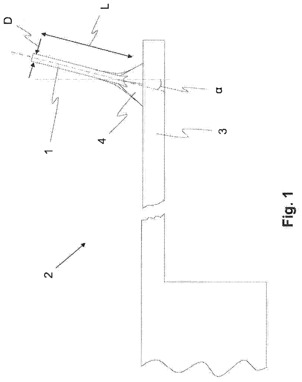
[0041]FIG. 1 shows a schematic side view of a probe device 2 having a tip 1 on a cantilever 3. The probe device 2 can be used for scanning probe microscopy. The probe device 2 can also be used for atomic force microscopy. According to the present embodiment, the tip 1 has an angle a with respect to a perpendicular to the cantilever 3. Alternatively, the tip 1 can also be arranged vertically on the cantilever 3. Furthermore, the tip 1 can be arranged on a tip base 4 on the cantilever 3. The tip base 4 can be pyramid-shaped, for example. By means of the tip base 4, the tip 1 can be arranged more stably on the cantilever 3.

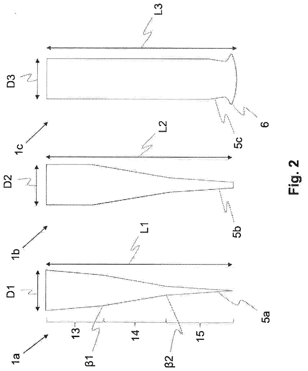
[0042]The tip 1 also has a length L. In addition, the tip 1 has a thickness D. For example, the length L can be in the range of a few hundred nanometers, and the thickness D in the range of a few tens of nanometers, for example between 3 nanometers and 20 nanometers. The length L of the tip 1 can also be a few, for example 10, micrometers. A cross-section of the tip ...


PUM

PropertyMeasurementUnit
depthaaaaaaaaaa
lengthaaaaaaaaaa
lengthaaaaaaaaaa

Abstract

The invention relates to a method for providing a probe device for scanning probe microscopy, in particular for atomic force microscopy, wherein a scanning probe microscope is used for measuring a sample by means of a tip which is arranged on a cantilever of the probe device and which has a tip geometry. According to the invention, in a step upstream of the manufacturing process producing the tip, the tip geometry is optimized based on a selected tip basic form with regard to defined, required measurement properties, by computer simulating and evaluating the tip geometry, and modifying the tip geometry according to the evaluation with regard to these measurement properties. The invention further relates to a probe device for scanning probe microscopy, in particular for atomic force microscopy, having a cantilever and a tip formed on the cantilever in the nanometer range, with which samples to be measured can be scanned.

Description

PRIORITY CLAIMS[0001]This application claims priority to PCT application PCT / EP2018 / 081016 filed Nov. 13, 2018, which claims priority to German Patent Application Number 10 2017 127 645.9 filed Nov. 23, 2017.FIELD OF THE INVENTION[0002]The present invention relates to a method for providing a probe device for scanning probe microscopy, in particular for atomic force microscopy, wherein a scanning probe microscope is used for measuring a sample by means of a tip which has a tip geometry and which is arranged on a cantilever of the probe device.BACKGROUND OF THE INVENTION[0003]Scanning probe microscopy and / or atomic force microscopy can be used, for example, to scan semiconductor components and structures arranged therein for quality assurance. The structures can include, for example, trenches and / or holes in the semiconductor component, which can have a width and / or a diameter of a few tens of nanometers and a depth of a several hundred nanometers. For example, in order to be able to...

Claims


Application Information

Patent Timeline
Patent Type & Authority Applications(United States)
IPC IPC(8): G01Q30/04G01Q70/16G01Q70/10
CPCG01Q70/16G01Q30/04G01Q70/14G01Q70/10
Inventor IRMER, BERND
Owner NANOTOOLS
Why Eureka
Try Eureka