Array substrate and display panel
- Summary
- Abstract
- Description
- Claims
- Application Information
AI Technical Summary
Benefits of technology
Problems solved by technology
Method used
Image

Examples
Embodiment Construction
[0035]In the description of the present disclosure, it should be understood that terms such as “center,”“longitudinal,”“lateral,”“length,”“width,”“thickness,”“upper,”“lower,”“front,”“rear,”“left,”“right,”“vertical,”“horizontal,”“top,”“bottom,”“inside,”“outside,”“clockwise,”“counter-clockwise” as well as derivative thereof should be construed to refer to the orientation as then described or as shown in the drawings under discussion. These relative terms are for convenience of description, do not require that the present disclosure be constructed or operated in a particular orientation, and shall not be construed as causing limitations to the present disclosure.
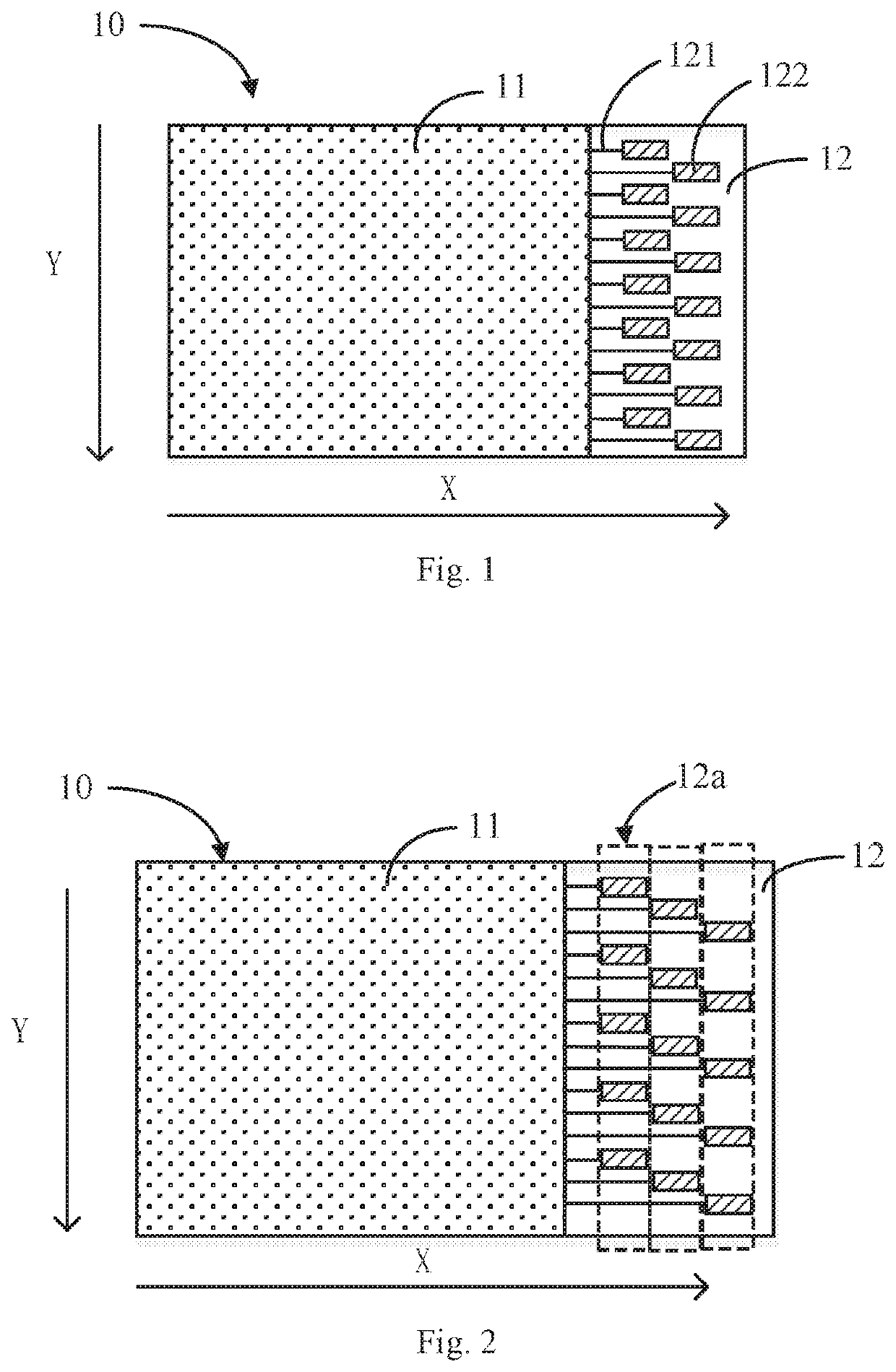
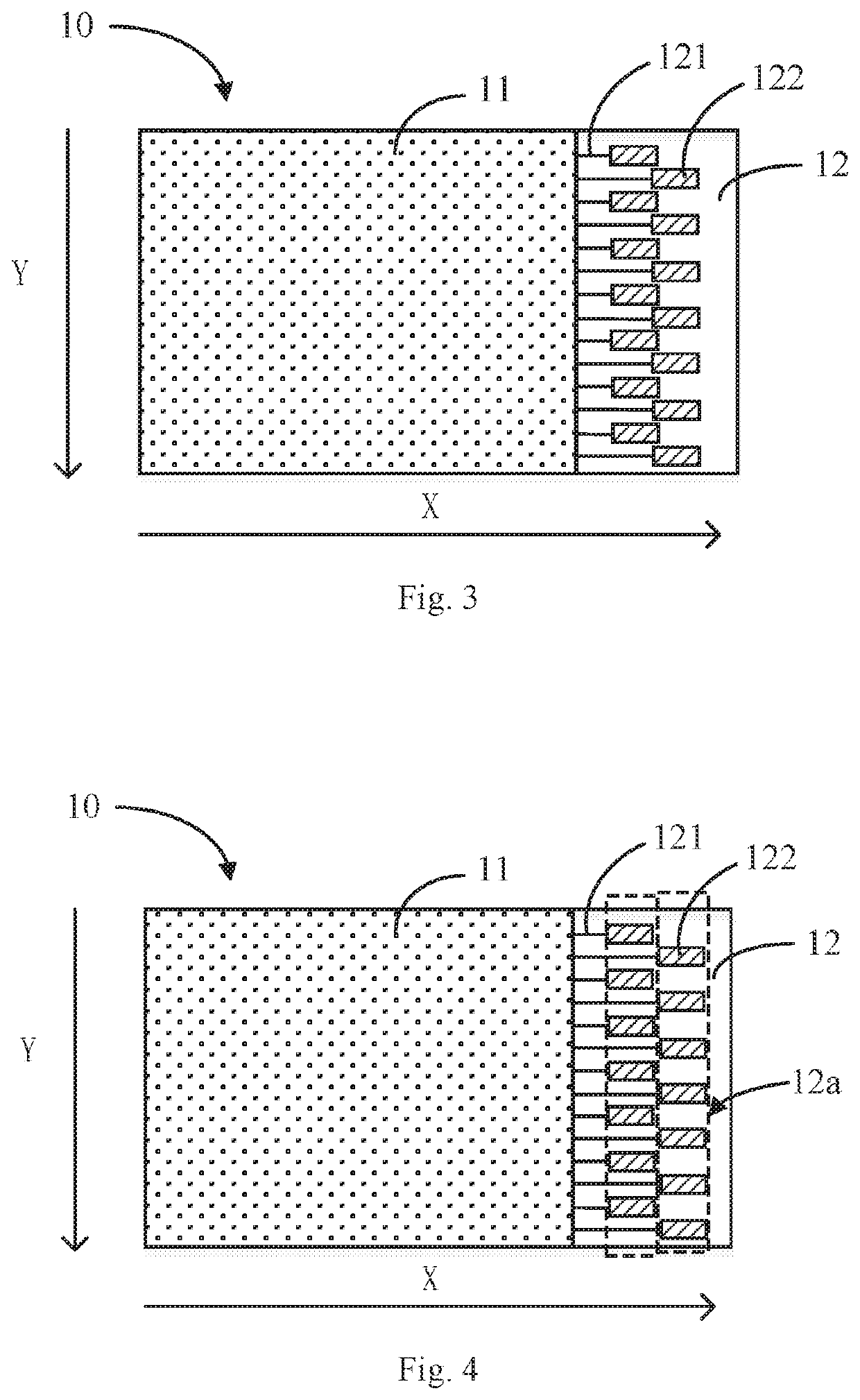
[0036]In order to resolve the problem that the spacing between connection terminals on the array substrate is excessively small, and short circuiting tends to happen when bonding to cause poor bonding in the related art, the embodiments of the present disclosure can resolve the above problem.
[0037]A description is provided with...
PUM
 Abstract
Description
Claims
Application Information
 - R&D Engineer
- R&D Manager
- IP Professional
- Industry Leading Data Capabilities
- Powerful AI technology
- Patent DNA Extraction
Browse by: Latest US Patents, China's latest patents, Technical Efficacy Thesaurus, Application Domain, Technology Topic.
© 2024 PatSnap. All rights reserved.Legal|Privacy policy|Modern Slavery Act Transparency Statement|Sitemap