Display panel and manufacturing method thereof

Active Publication Date: 2020-11-19
AU OPTRONICS CORP
View PDF0 Cites 0 Cited by
  • Summary
  • Abstract
  • Description
  • Claims
  • Application Information

AI Technical Summary

Benefits of technology

The invention provides a display panel that can show a black image without any reduction in display quality. This is achieved by making the first data line of the array substrate electrically connected to the common line, so that a common voltage can be supplied to the first data line. By controlling the common potentials of the opposite substrate and the array substrate, the first pixel unit can be in a dark state. This prevents any issues related to the cut portion of the display panel.

Problems solved by technology

However, designing the mask is expensive.
Cutting the display with the large size may cause fanout line to be cut off such that the pixel units cannot be controlled.

Method used


Image

  • Display panel and manufacturing method thereof
  • Display panel and manufacturing method thereof
  • Display panel and manufacturing method thereof

Examples


Embodiment Construction

[0021]Reference will now be made in detail to the present embodiments of the invention, examples of which are illustrated in the accompanying drawings. Wherever possible, the same reference numbers are used in the drawings and the description to refer to the same or like parts.

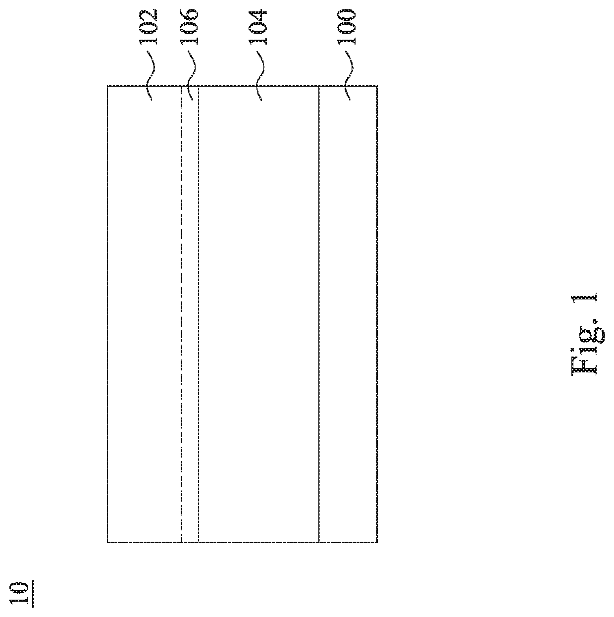
[0022]FIG. 1 is a cross-sectional view of a display panel 10 according to one embodiment of the present invention. Reference is made to FIG. 1. The display panel 10 includes a mother board 100, an opposite substrate 102, and a liquid crystal layer 104. In the present embodiment, the opposite substrate 102 is a substrate including an opposite electrode 106. The liquid crystal layer 104 is disposed between the mother board 100 and the opposite substrate 102. The display panel 10 of the present invention can be any kind of liquid crystal display pane, for example, but is not limited to, a polymer stabilized alignment (PSA) liquid crystal display panel. The opposite substrate 102 may include, but is not limited to...


PUM


Abstract

A display panel includes an array substrate, a first pixel unit, a first data line, a common line, a first fanout line, and an opposite substrate. The array substrate includes a substrate including a first display region, a second display region, and a non-display region. The second display region includes a first side and a second side connected to the first side. The non-display region is adjacent connected to the first side. The first display region is adjacent connected to the second side. The first display region has a third side opposite to the second side. The third side is substantially aligned with an edge of the substrate. A first fanout line is disposed on the non-display region and connected to the first data line. The first fanout line has an end substantially aligned with the edge of the substrate.

Description

CROSS-REFERENCE TO RELATED APPLICATION[0001]This application claims priority to Taiwan Application Serial Number 108116784, filed May 15, 2019, which is herein incorporated by reference in its entirety.BACKGROUNDField of Invention[0002]The present invention relates to a display panel and a manufacturing method thereof.Description of Related Art[0003]In terms of displays, a thin-film transistor liquid crystal display (TFT-LCD) having high resolution, high space utilization efficiency and low power consumption and no radiation has gradually become mainstream market products.[0004]The thin-film transistor array substrate has a plurality of pixel units, scan lines and data lines arranged in an array. The thin-film transistor of each pixel unit is controlled by the corresponding scan line and data line. The data line and the scan line are connected to the source driving circuit and the gate driving circuit through fanout lines.[0005]Generally, methods of forming the thin-film transistor ...

Claims


Application Information

Patent Timeline
IPC IPC(8): G02F1/1362G02F1/1345H01L27/12
CPCG02F2001/136295H01L27/1259G02F1/136286G02F1/13452H01L27/124G02F1/1362G02F1/136295
Inventor SHIH, PING-HUNGHSIEH, MENG-TING
Owner AU OPTRONICS CORP
Why Eureka
Try Eureka