El display apparatus

a technology of display apparatus and display panel, which is applied in the direction of electrical apparatus, semiconductor devices, instruments, etc., can solve the problems of display irregularities, and difficulty in realizing large-scale and high-definition display panel, and achieve sufficient charging/discharging parasitic capacitance, the effect of satisfying the image display

Inactive Publication Date: 2020-12-17
JOLED INC
View PDF0 Cites 2 Cited by
  • Summary
  • Abstract
  • Description
  • Claims
  • Application Information

AI Technical Summary

Benefits of technology

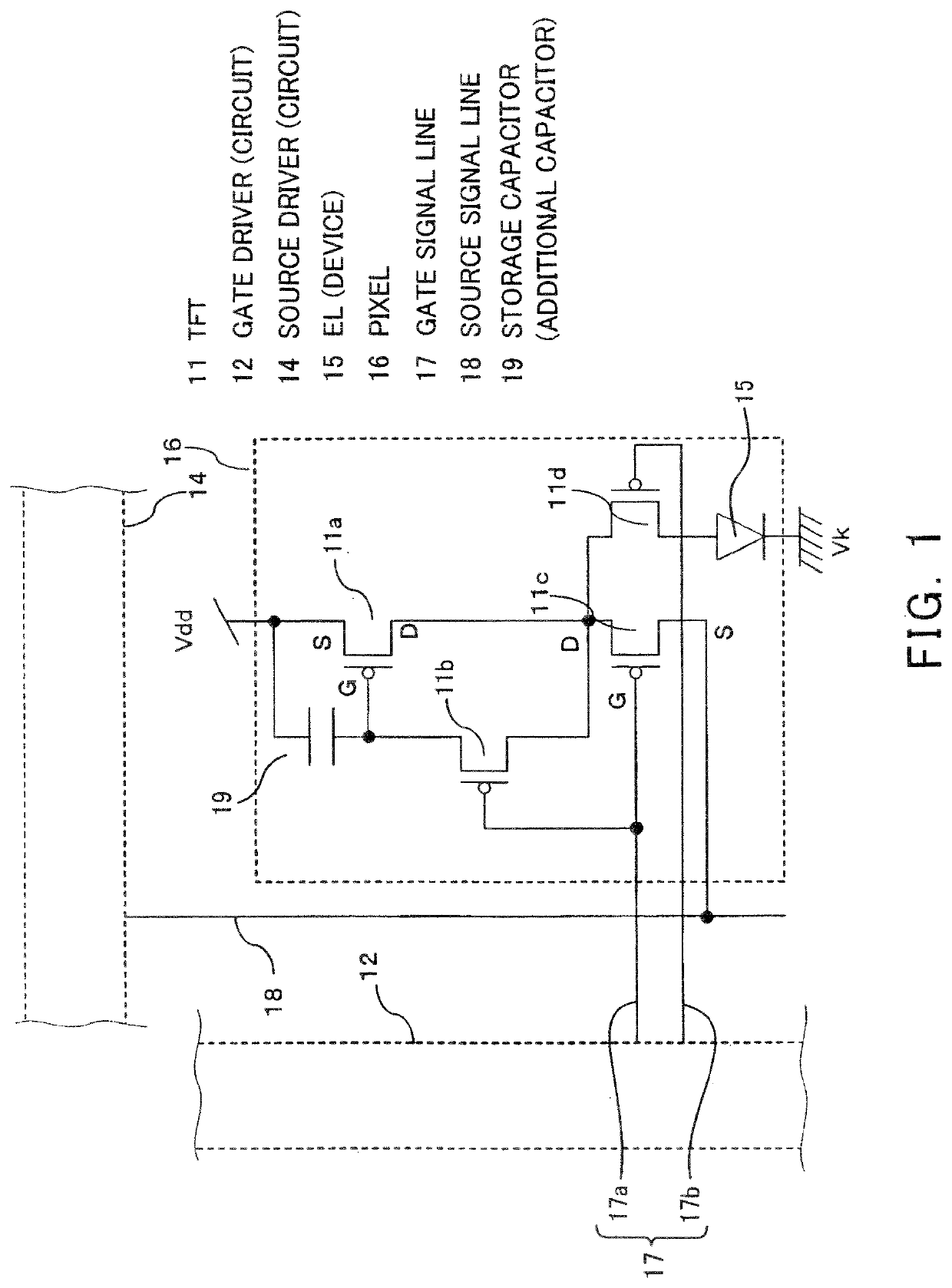
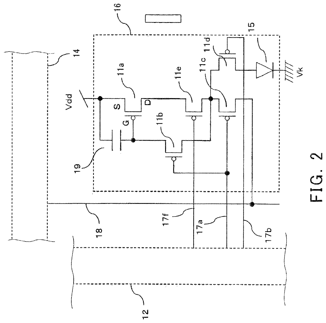
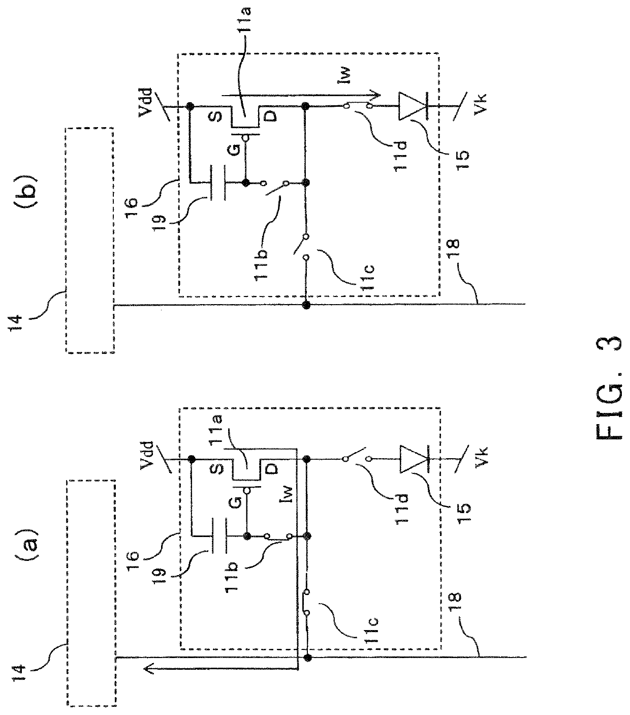
[0015]The present invention has been made in view of the foregoing circumstances. It is an object of the present invention to provide an EL display apparatus which is capable of realizing satisfactory image display by sufficiently charging / discharging the parasitic capacitance present in the source signal line.

Problems solved by technology

Though the former configuration is simple in structure, it has a difficulty in realizing a large-scale and high-definition display panel.
However, it has problems of a technical difficulty in control and of a relatively high price.
Since organic EL devices emit light based on current, the organic EL display panel involves a problem that display irregularities occur if there are variations in transistor characteristics.
Further, a conventional EL display panel cannot sufficiently charge / discharge the parasitic capacitance which is present in the source signal line 18.
For this reason there arises a problem that in some cases a desired current cannot be fed to pixel 16.

Method used


Image

  • El display apparatus
  • El display apparatus
  • El display apparatus

Examples


Embodiment Construction

[0105]Hereinafter, embodiments of the present invention will be described with reference to the drawings.

[0106]For easy understanding and / or illustration, each of the drawings in this description may have portions omitted and / or enlarged / reduced. For example, an encapsulating film 111 and the like are shown to be quite thick in the sectional view of a display panel at FIG. 11. On the other hand, an encapsulating cover 85 is shown to be thin in FIG. 10. There are omitted portions. For example, a display panel or the like according to the present invention needs to have a phase film such as a circularly polarizing plate for antireflection. However, such a phase film is omitted from the drawings used in this description. This holds true for other drawings. Like numerals, characters or the like designate parts having identical or similar forms, materials, functions or operations.

[0107]It is to be noted that the details to be described with reference to the drawings may be combined with ...


PUM


Abstract

An EL display apparatus is provided. A display screen includes pixels arranged in a matrix, with each pixel including an EL device and a pixel circuit. A source driver circuit is configured to output an analog video signal to each pixel. A gate driver circuit is on at least one side of the display screen, with the gate driver circuit including first and second gate driver circuits. Each pixel includes a driving transistor, a first switch transistor, and a second switch transistor. A gate terminal of the first switch transistor is connected to a first gate signal line of the first gate driver circuit, and a gate terminal of the second switch transistor is connected to a second gate signal line of the second gate driver circuit. The first and second switch transistors are on/off controlled, independently, by the first and second gate driver circuits.

Description

RELATED APPLICATIONS[0001]This application is a Continuation of U.S. patent application Ser. No. 16 / 861,676, filed Apr. 29, 2020, which is a Continuation of U.S. patent application Ser. No. 16 / 714,206, filed Dec. 13, 2019 and now U.S. Pat. No. 10,699,639 issued Jun. 30, 2020, which is a Continuation of U.S. patent application Ser. No. 16 / 152,999, filed Oct. 5, 2018 and now U.S. Pat. No. 10,553,158 issued Feb. 4, 2020, which is a Continuation of U.S. patent application Ser. No. 15 / 335,901, filed Oct. 27, 2016 and now U.S. Pat. No. 10,134,336 issued Nov. 20, 2018, which is a Continuation of U.S. patent application Ser. No. 14 / 341,620, filed Jul. 25, 2014 and now U.S. Pat. No. 9,728,130 issued Aug. 8, 2017, which is a Continuation of U.S. patent application Ser. No. 10 / 488,591, filed Sep. 17, 2004 and now U.S. Pat. No. 8,823,606 issued Sep. 2, 2014, which is a U.S. National Phase under 35 U.S.C. § 371 of International Application No. PCT / JP2002 / 009111, filed Sep. 6, 2002, which in turn...

Claims


Application Information

Patent Timeline
Patent Type & Authority Applications(United States)
IPC IPC(8): G09G3/3241H01L27/32G09G3/325G09G3/3266G09G3/32H01L27/12H01L51/52G09G3/3233G09G3/3258G09G3/20G09G3/3275G09G5/02
CPCG09G2310/0289G09G3/325H01L27/1255H05K999/99G09G2320/0646G09G2310/0218H01L51/5259G09G3/32H01L27/3262G09G3/2003G09G2320/043H01L27/3244G09G2310/0256G09G2320/0626G09G3/3258H01L33/58H01L27/156G09G2320/0247G09G2300/0852H01L51/5253G09G3/3266H01L51/5281G09G2310/0205H01L27/3211H01L27/3265G09G2320/0653G09G2300/0809G09G2320/0261G09G2300/0861H01L27/3216G09G2310/027G09G3/2007G09G3/3233H01L51/525G09G2300/0413G09G2320/06H01L27/1251G09G2310/08G09G3/3241G09G2320/0257H01L29/78645G09G2310/0251G09G3/3275G09G2300/0814G09G2320/0606G09G2300/0404G09G2310/0248H01L29/78672G09G2300/0819H01L33/56H01L27/124G09G5/02H01L27/127G09G2300/0842H10K59/126H10K59/12G09G3/30H10K50/846H10K50/8428H10K59/35H10K59/1213H10K59/1216H10K50/86H10K50/844H10K59/352
Inventor TAKAHARA, HIROSHITSUGE, HITOSHI
Owner JOLED INC
Why Eureka
Try Eureka