Multilayer wiring base plate and probe card using the same

a multi-layer wiring and probe card technology, applied in the direction of base element modifications, circuit inspection/indentification, instruments, etc., can solve the problem of accelerate deterioration of thin-film resistors, and achieve the effect of efficiently dissipating heat generated by thin-film resistors

Active Publication Date: 2020-12-24
NIHON MICRONICS
View PDF0 Cites 0 Cited by
  • Summary
  • Abstract
  • Description
  • Claims
  • Application Information

AI Technical Summary

Benefits of technology

[0022]According to the present invention, in a multilayer wiring base plate incorporating a thin-film resistor, heat generated from the thin-film resistor can be dissipated efficiently.

Problems solved by technology

Such repeated stresses caused by the temperature changes may accelerate deterioration of the thin-film resistor and cause breakage.

Method used


Image

  • Multilayer wiring base plate and probe card using the same
  • Multilayer wiring base plate and probe card using the same
  • Multilayer wiring base plate and probe card using the same

Examples


modification example 1

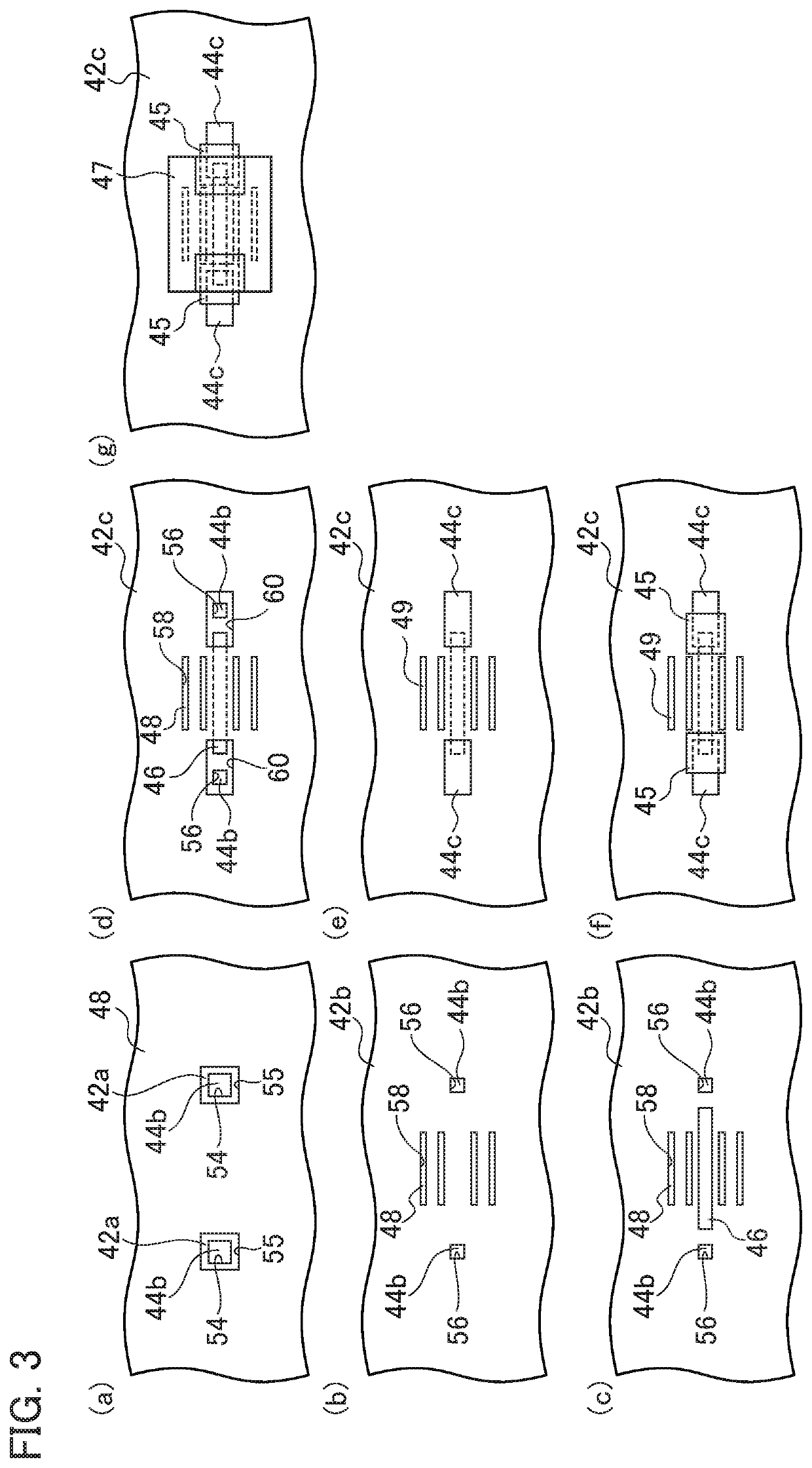
[0095]In the embodiment of the present invention, although the probe card 10 in which two pairs of heat dissipation and pedestal connecting portions 49 (49a, 49b, 49c, and49d) are provided on both the lateral sides of the thin-film resistor 46 along the longitudinal direction of the thin-film resistor 46 has been illustrated and described, the present invention is not limited to this.

[0096]In Modification Example 1, the probe card 10 including the multilayer wiring base plate in which the heat dissipation and pedestal connecting portions provided on each side are connected to enable heat conduction will be illustrated and described.

[0097]FIG. 4(a) is a plan view of a part provided with one thin-film resistor of the multilayer wiring base plate 38 included in the probe card 10 according to Modification Example 1 of the present invention, and FIG. 4(b) is a cross-sectional view cut along the cross-section C-C′ in FIG. 4(a).

[0098]As illustrated in FIGS. 4(a) and 4(b), the heat dissipat...

modification example 2

[0104]In the embodiment of the present invention, although the probe card 10 has been illustrated and described including the multilayer wiring base plate including the insulating protecting layers 45 provided to cover parts, that is, opposed inner parts, of the paired connecting electrodes 44c projecting from the insulating plate 41 and the heat dissipating portion 47 provided to cover the paired insulating protecting layers 45 and the third synthetic resin layer 42c provided between the paired insulating protecting layers 45 without contacting the paired connecting electrodes 44c, the present invention is not limited to this.

[0105]In Modification Example 2 of the present invention, the probe card 10 will be illustrated and described including the multilayer wiring base plate including an insulating protecting layer 45A provided to cover the parts of the paired connecting electrodes 44c projecting from the insulating plate 41 and the third synthetic resin layer 42c provided between...

modification example 3

[0109]In Modification Example 3 of the present invention, the probe card 10 will be illustrated and described including the multilayer wiring base plate including an insulating protecting layer provided to cover the entireties of the paired connecting electrodes 44c projecting from the insulating plate 41 and the upper part of the insulating plate 41 between the paired connecting electrodes 44c.

[0110]FIG. 6(a) is a plan view of a part provided with one thin-film resistor of the multilayer wiring base plate 38 included in the probe card 10 according to Modification Example 3 of the present invention, and FIG. 6(b) is a cross-sectional view cut along the cross-section A-A′ in FIG. 6(a).

[0111]As illustrated in FIGS. 6(a) and 6(b), an insulating protecting layer 45B is provided to cover the entireties of the paired connecting electrodes 44c projecting from the insulating plate 41 and the upper part of the insulating plate 41 between the paired connecting electrodes 44c. The heat dissip...


PUM

PropertyMeasurementUnit
heat conductivityaaaaaaaaaa
electrical testaaaaaaaaaa
impedanceaaaaaaaaaa

Abstract

Included are an insulating plate 41 including a plurality of insulating synthetic resin layers, wiring circuits 44a, 44b, and 44c provided in the insulating plate 41, a thin-film resistor 46 formed to be buried in the insulating plate 41 and electrically connected to the wiring circuits 44a, 44b, and 44c, a heat dissipating portion 47 provided over one surface of the insulating plate to be opposed to the thin-film resistor 46 via a part of the plurality of insulating synthetic resin layers and having higher heat conductivity than that of the insulating plate 41, a pedestal portion 48 formed to be buried in the insulating plate 41 and provided to be opposed to the thin-film resistor 46 via a part of the plurality of insulating synthetic resin layers on an opposite side of the heat dissipating portion 47 and having higher heat conductivity than that of the insulating plate 41, and a heat dissipation and pedestal connecting portion 49 connecting the heat dissipating portion 47 to the pedestal portion 48 and having higher heat conductivity than that of the insulating plate 41.

Description

TECHNICAL FIELD[0001]The present invention relates to a multilayer wiring base plate interposed on an electrical path between a device under test and a tester to transmit a signal required for a test and incorporating a thin-film resistor and a probe card using the multilayer wiring base plate.BACKGROUND ART[0002]Semiconductor integrated circuits (hereinbelow referred to as “wafer chips” as well) collectively formed on a semiconductor wafer (hereinbelow referred to simply as “a wafer” as well) undergo an electrical test (for example, a wafer test) with use of a tester apparatus (hereinbelow referred to as “a tester” as well) before being separated into respective chips. In general, for this electrical test is used a probe card interposed between the tester and each of the wafer chips serving as a device under test to transmit a test signal, a response output, and the like between the tester and the device under test. Respective probes of the probe card connected to the tester are br...

Claims


Application Information

Patent Timeline
Patent Type & Authority Applications(United States)
IPC IPC(8): G01R31/28G01R1/073H05K1/02H05K1/16
CPCH05K2201/0317G01R31/2818G01R1/073H05K2201/068H05K1/167H05K1/0266G01R1/07378H05K1/0206H05K1/0298G01R1/07307G01R1/20G01R31/2886H05K1/0203
Inventor OTABE, NOBORUFUKAMI, YOSHIYUKI
Owner NIHON MICRONICS
Why Eureka
Try Eureka