Method For Manufacturing Led Display

a technology of led display and manufacturing method, which is applied in the direction of identification means, instruments, semiconductor/solid-state device testing/measurement, etc., can solve the problem that the height of the bonding conductive member is likely to vary

Inactive Publication Date: 2020-12-24
V TECH CO LTD
View PDF0 Cites 2 Cited by
  • Summary
  • Abstract
  • Description
  • Claims
  • Application Information

AI Technical Summary

Benefits of technology

[0007]According to the method for manufacturing an LED display of the present invention, the stop layers restrict the compression of the elastic support members when the LED substrate pressed and joined onto the wiring board. Thus, the LEDs are permanently bonded onto the wiring board with the LEDs arranged at a constant distance from the wiring board.

Problems solved by technology

However, such bonding conductive members are likely to vary in height when they are pressed.

Method used


Image

  • Method For Manufacturing Led Display
  • Method For Manufacturing Led Display
  • Method For Manufacturing Led Display

Examples


Embodiment Construction

[0031]Hereinafter, an embodiment of the present invention will be described in detail with reference to the accompanying drawings.

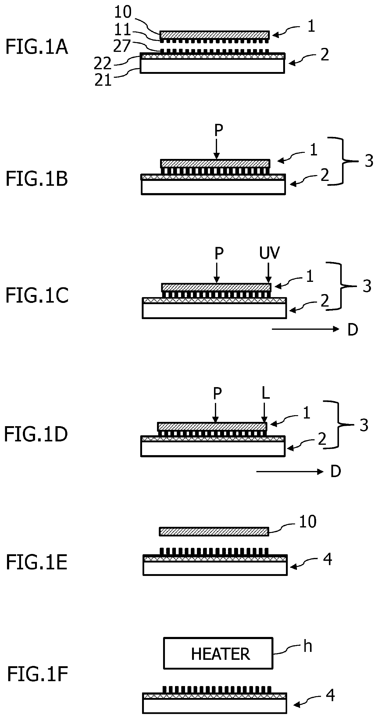
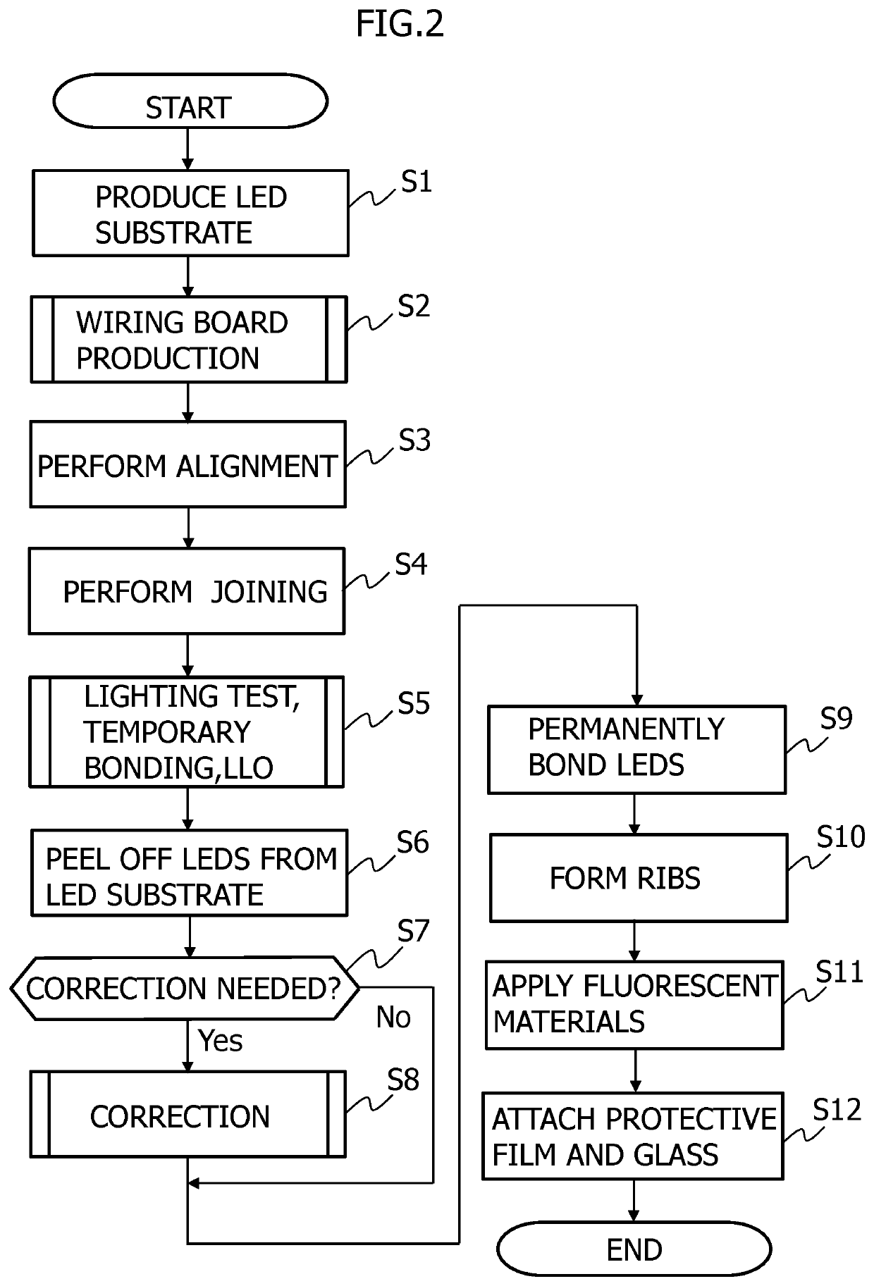
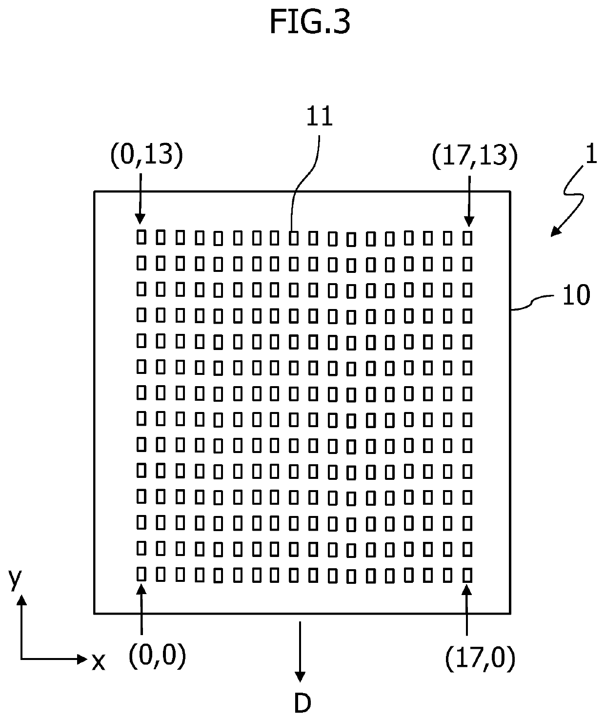
[0032]FIGS. 1A to 1F are diagrams illustrating a method for manufacturing an LED display according to the present invention. FIG. 2 is a flowchart showing steps of the method for manufacturing an LED display according to the present invention. In the following description, it is assumed that each micro LED has external dimensions, for example, of 10 μm or less×30 μm or less. Furthermore, each of the micro LEDs in the LED display manufactured by the method has passed a lighting test, which will be described later, and thus is proved to have favorable light emission characteristics. Here, a major application of the method for manufacturing an LED display according to the present invention is manufacture of LED displays using micro LEDs. However, the method for manufacturing an LED display according to the present invention may also be applicable to manufact...


PUM

PropertyMeasurementUnit
wavelengthaaaaaaaaaa
heightaaaaaaaaaa

Abstract

The present invention provides a method for manufacturing an LED display including a wiring board and LEDs arranged at a constant distance from the wiring board. The method includes: aligning an LED substrate 1 having LEDs 11 with a wiring board 2, and pressing and joining the LED substrate onto the wiring board. Each LED has a bonding surface. The wiring board includes bonding layers. The aligning step is performed so that the bonding surfaces are joined on the bonding layers in the pressing and joining step. The method further includes: temporarily bonding the LEDs onto the wiring board by curing the bonding layers through irradiation with ultraviolet light UV; peeling off the LEDs from the LED substrate through irradiation with laser light L; and permanently bonding the LEDs onto the wiring board by heating the bonding layers of the LEDs so as to further cure the bonding layers.

Description

[0001]This application is a continuation application of PCT / JP2019 / 001419, filed on Jan. 18, 2019.TECHNICAL FIELD[0002]The present invention relates to a method for manufacturing a light emitting diode (LED) display, and more particularly, relates to a method for manufacturing an LED display in which LEDs are mounted on a wiring board with elastic support members interposed therebetween so that the LEDs are arranged at a constant distance from the wiring board.BACKGROUND ART[0003]Conventionally known examples of image display devices include an image display device having an LED array in which LEDs are arranged in a matrix (see Patent Document 1, for example). The process of manufacturing such an image display device includes: providing a sapphire substrate on which LEDs formed; and mounting the LEDs onto a wiring board by peeling off the LEDs from the sapphire substrate, for example. According to Patent Document 1, in the mounting step, the electrodes of the LEDs are conductively b...

Claims


Application Information

Patent Timeline
Patent Type & Authority Applications(United States)
IPC IPC(8): H01L21/66H01L25/16H01L23/00
CPCH01L22/22H01L2224/83874H01L25/167H01L2224/83885H01L24/83H01L2224/83005H01L2924/12041H01L2224/83862H01L2224/83859H01L2924/1033G09F9/00G09F9/30G09F9/33H01L21/6835H01L22/14H01L22/20H01L24/29H01L24/32H01L24/92H01L24/95H01L24/98H01L2221/68318H01L2221/68363H01L2221/68381H01L2224/2919H01L2224/32225H01L2224/83001H01L2224/8312H01L2224/83192H01L2224/83203H01L2224/83908H01L2224/83986H01L2224/95001H01L33/00H01L33/005
Inventor YANAGAWA, YOSHIKATSUFUKAYA, KOICHIROOKURA, NAOYA
Owner V TECH CO LTD
Why Eureka
Try Eureka