Semiconductor package

a semiconductor and package technology, applied in the field of semiconductor packages, can solve the problems of product failure, interference with dram, electromagnetic waves emitted by other surrounding electronic products, etc., and achieve the effect of preventing electromagnetic interference (emi) between the semiconductor package and other surrounding electronic products and further improving the electromagnetic sensibility of the semiconductor packag

Inactive Publication Date: 2021-02-04
NAN YA TECH
View PDF4 Cites 0 Cited by
  • Summary
  • Abstract
  • Description
  • Claims
  • Application Information

AI Technical Summary

Benefits of technology

[0025]In the aforementioned embodiments of the present disclosure, since the dummy die is disposed on the semiconductor die, and the conductive layer is disposed on the dummy die to be electrically connected to the ground reference by the second conductive wire, electromagnetic waves generated by the semiconductor die are blocked from interfering with other surrounding electronic devices, and thus the electromagnetic interference (EMI) between the semiconductor package and other surrounding electronic products is prevented. Additionally, the electromagnetic sensibility (EMS) of the semiconductor package is further improved.

Problems solved by technology

When a dynamic random access memory (DRAM) is in operation, electromagnetic waves, which cause interference with other surrounding electronic products, are generated due to electromagnetic effects, and thus resulting in product failure.
On the other hand, electromagnetic waves emitted by other surrounding electronic products also interfere with the DRAM.

Method used


Image

  • Semiconductor package
  • Semiconductor package
  • Semiconductor package

Examples


Embodiment Construction

[0036]Reference will now be made in detail to the present embodiments of the disclosure, examples of which are illustrated in the accompanying drawings. Wherever possible, the same reference numbers are used in the drawings and the description to refer to the same or like parts.

[0037]In the embodiments of the present disclosure, a semiconductor package and a method of manufacturing the same are provided. For the purpose of simplicity and clarity, the method of manufacturing the semiconductor package will be described first in the article. Furthermore, some of the secondary elements may be omitted in the drawings accompanying the following embodiments.

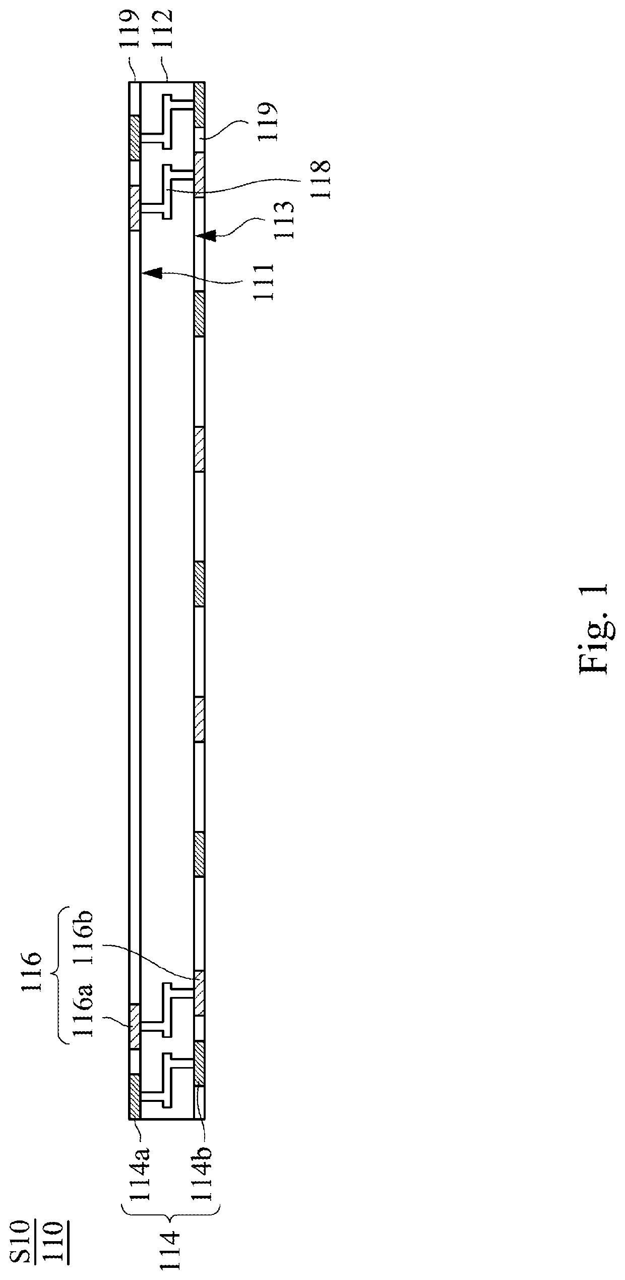
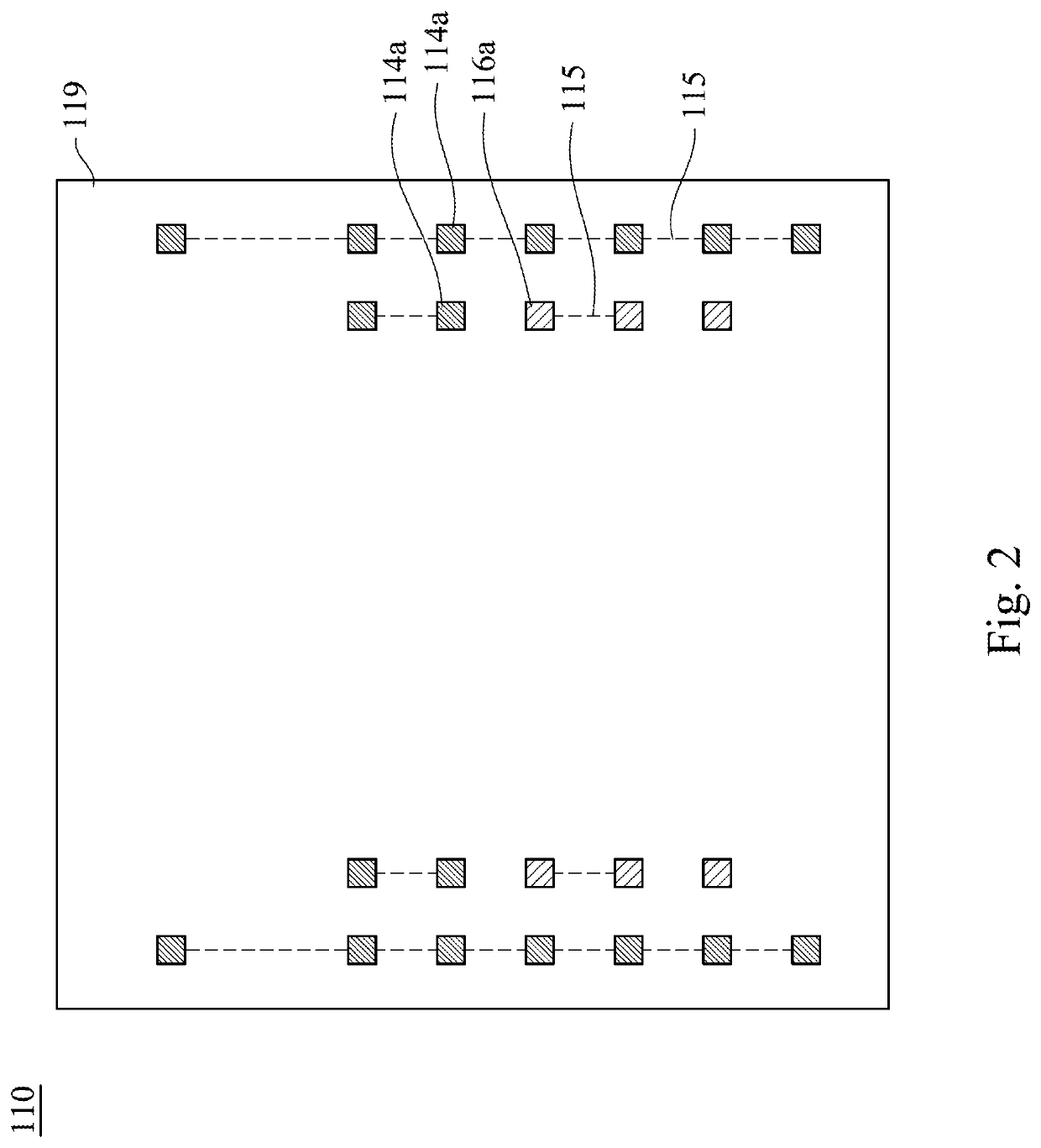
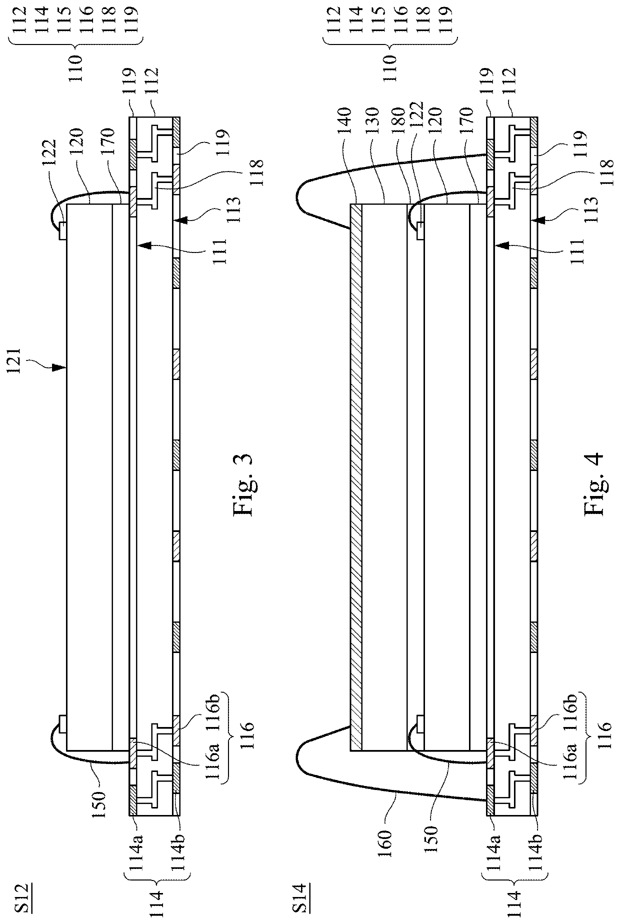
[0038]Reference is made to FIGS. 1 and 2, which are a cross-sectional view and a top view of step S10 of forming a semiconductor package 100 of FIG. 5. In step S10, a dielectric layer 112 having a first surface 111 and a second surface 113 is provided. A plurality of first conductive pads 114, a plurality of traces 115, and a plurality ...


PUM

PropertyMeasurementUnit
conductiveaaaaaaaaaa
vertical projection areaaaaaaaaaaa
semiconductoraaaaaaaaaa

Abstract

A semiconductor package includes a substrate, a semiconductor die, a dummy die, a conductive layer, at least one first conductive wire, and at least one second conductive wire. The semiconductor die is disposed on the substrate. The dummy die is disposed on the semiconductor die. The conductive layer is disposed on the dummy die. The first conductive wire electrically connects the semiconductor die to a signal source. The second conductive wire electrically connects the conductive layer to a ground reference.

Description

BACKGROUNDField of Invention[0001]The present disclosure relates to a semiconductor package.Description of Related Art[0002]When a dynamic random access memory (DRAM) is in operation, electromagnetic waves, which cause interference with other surrounding electronic products, are generated due to electromagnetic effects, and thus resulting in product failure. This phenomenon is referred to as an electromagnetic interference (EMI). On the other hand, electromagnetic waves emitted by other surrounding electronic products also interfere with the DRAM.[0003]As such, it is desirable to develop a DRAM device with an improved anti-interference ability, also referred to as an electromagnetic sensibility (EMS), to prevent electromagnetic interference.SUMMARY[0004]The present disclosure relates in general to a semiconductor package.[0005]According to an embodiment of the present disclosure, a semiconductor package includes a substrate, a semiconductor, a dummy die, a conductive layer, at least...

Claims


Application Information

Patent Timeline
Patent Type & Authority Applications(United States)
IPC IPC(8): H01L23/552H01L23/00H01L23/498H01L23/31
CPCH01L23/552H01L24/48H01L24/33H01L24/73H01L23/49816H01L2924/1436H01L23/3128H01L2224/73265H01L2224/73215H01L2224/33181H01L23/49827H01L23/3121H01L23/535H01L23/147H01L23/49838H01L23/49833H01L23/49822H01L23/13H01L2224/4824H01L2924/181H01L24/32H01L2224/32225H01L2224/32145H01L2924/15311H01L2224/48091H01L2224/05554H01L2224/06151H01L2224/48227H01L2224/49176H01L24/49H01L24/05H01L24/06H01L2224/04042H01L2924/3025H01L2224/92247H01L2224/92165H01L24/83H01L24/85H01L24/92H01L2224/05624H01L2924/15151H01L2224/8592H01L2224/81447H01L2224/45144H01L2924/00012H01L2924/00014H01L2924/00
Inventor HSIEH, CHANG-CHUN
Owner NAN YA TECH
Why Eureka
Try Eureka