
Device and method for disturbance free 3D MRAM fabrication

a technology of disturbance free and fabrication method, which is applied in the direction of magnetic field-controlled resistors, semiconductor devices, electrical equipment, etc., can solve the problems of affecting the integration level of mram, affecting the reliability of mram, and difficult connecting the fixed layer and the free layer, so as to improve the reliability and the integration level. the effect of higher level

Active Publication Date: 2022-02-22
SEMICON MFG INT (SHANGHAI) CORP +1
View PDF62 Cites 0 Cited by
  • Summary
  • Abstract
  • Description
  • Claims
  • Application Information

AI Technical Summary

Benefits of technology

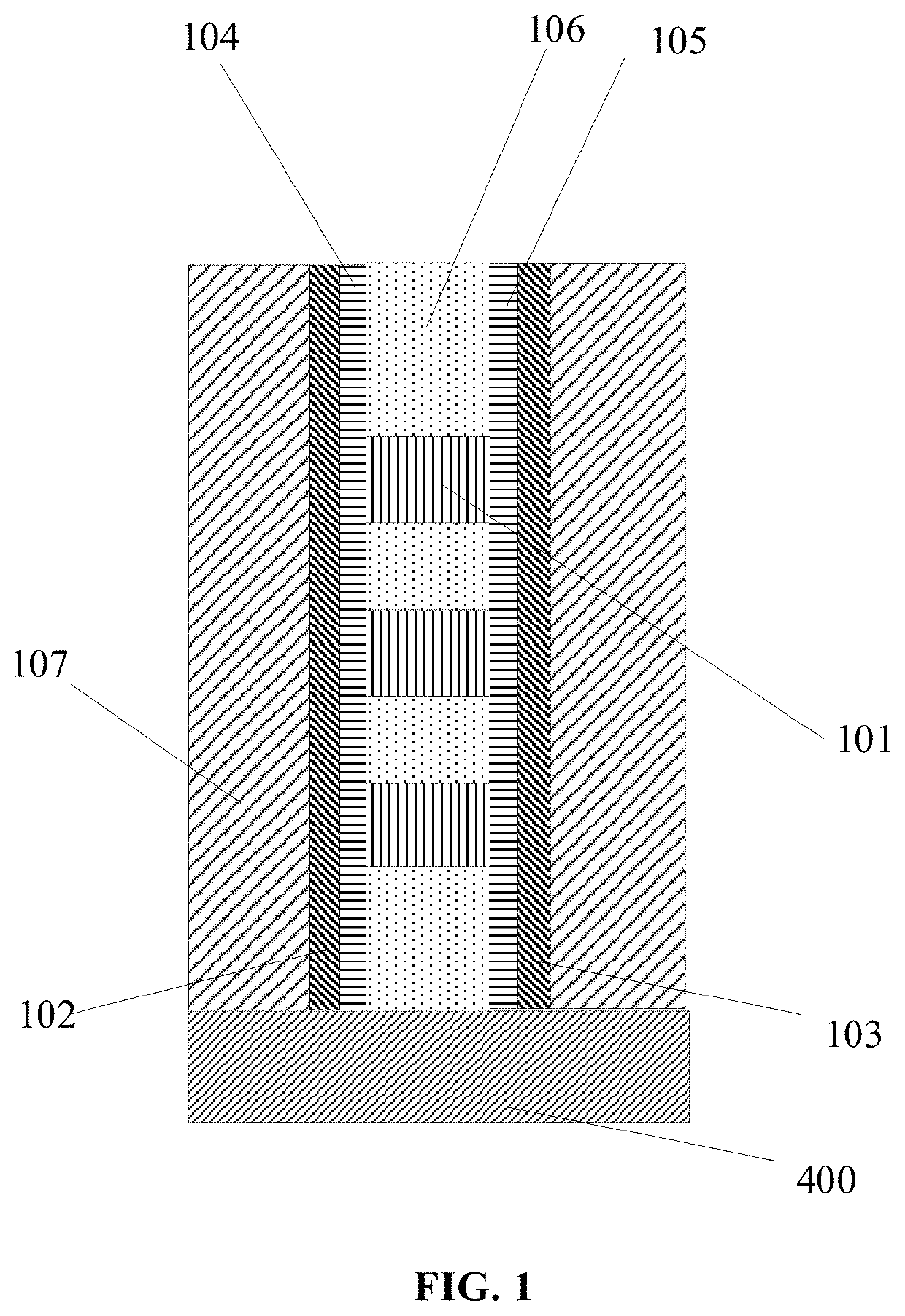
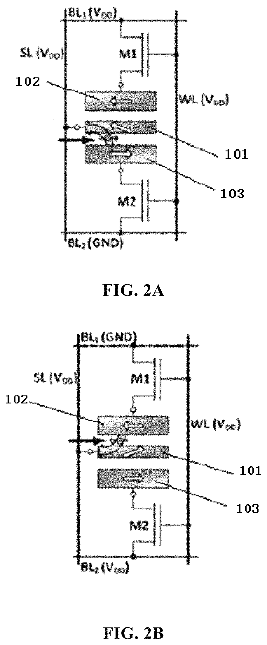
[0005]Embodiments of the present invention provide a magnetic memory cell, a magnetic random access memory with improved reliability and higher level of integration, and a method for manufacturing thereof.
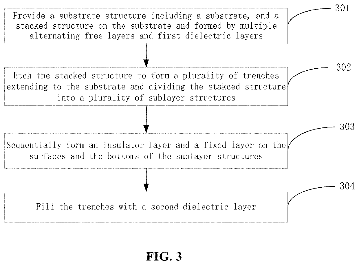
[0022]A magnetic random access memory manufactured by the above-described method of the present invention includes a first fixed layer and a second fixed layer that are shared by a plurality of memory cells. The integration level can thus be increased and the electromagnetic interference between memory cells can be reduced.

Problems solved by technology

When the integration level of memory cells in an MRAM is high, the process of connecting the fixed layer and the free layer becomes relatively more difficult, which affects the integration level of the MRAM.
Further, with the high integration level of memory cells in an MRAM, and a voltage applied between the free layer and the fixed layer, the current flowing therethrough will cause magnetic field interference of the fixed layer and the free layer of neighboring memory cells, thereby adversely affecting the MRAM reliability.

Method used


Image

  • Device and method for disturbance free 3D MRAM fabrication
  • Device and method for disturbance free 3D MRAM fabrication
  • Device and method for disturbance free 3D MRAM fabrication

Examples


Embodiment Construction

[0029]In the following description, numerous specific details are provided for a thorough understanding of the present invention. However, it should be appreciated by those of skill in the art that the present invention may be realized without one or more of these details. In other examples, features and techniques known in the art will not be described for purposes of brevity.

[0030]It will be understood that the drawings are not drawn to scale, and similar reference numbers are used for representing similar elements. Embodiments of the invention are described herein with reference to functional block diagrams that are schematic illustrations of idealized embodiments (and intermediate structures) of the invention. For purposes of clarity, not every component may be labeled in every drawing.

[0031]It will be understood that, when an element or component is referred to as “connected to” or “coupled to” another element or component, it can be connected or coupled to the other element or...


PUM


Abstract

A magnetic random access memory includes a memory cell including a first fixed layer, a second fixed layer, and one or more free layers disposed between the first fixed layer and the second fixed layer. The first and second fixed layers are continuous layers and commonly shared by a plurality of memory cells. The magnetic random access memory has a relatively simple structure that not only reduces magnetic interference between memory cells, but also simplifies the fabrication process and increases the integration level.

Description

CROSS-REFERENCES TO RELATED APPLICATIONS[0001]This application claims priority to Chinese patent application No. 201710190486.3, filed with the State Intellectual Property Office of People's Republic of China on Mar. 28, 2017, the content of which is incorporated herein by reference in its entirety.FIELD OF THE INVENTION[0002]The present invention relates generally to semiconductor technology. More particularly, embodiments of the present invention relate to a magnetic random access memory cell, a random access memory including the memory cell, and a manufacturing method thereof.BACKGROUND OF THE INVENTION[0003]Magnetic random access memory (MRAM) refers to a random access memory that stores data based on magnetoresistive properties. It uses the different magnetic resistances due to the different magnetization directions to store “0” and “1” bits. As long as the external magnetic field does not change, the magnetization direction also does not change. With the increase in technical ...

Claims


Application Information

Patent Timeline
Patent Type & Authority Patents(United States)
IPC IPC(8): H01L27/22H01L43/02H01L43/08H01L43/12
CPCH01L27/228H01L43/02H01L43/08H01L43/12H10B61/00H10N50/80H10N50/01H10B61/22H10N50/10
Inventor SONG, YIBINCHEN, ZHUOFAN
Owner SEMICON MFG INT (SHANGHAI) CORP
Learn More