Display having infrared element arranged such that at least one portion thereof overlaps pixel, and electronic device including same

a technology of infrared elements and electronic devices, applied in the field of display, can solve the problems of low security level of security companies, cumbersome dealing with security companies, misrecognition of fingerprints, etc., and achieve the effects of reducing the sensing error rate of biometric sensors, increasing the precision of recognition, and high resolution

Active Publication Date: 2021-02-04
SAMSUNG ELECTRONICS CO LTD
View PDF0 Cites 8 Cited by
  • Summary
  • Abstract
  • Description
  • Claims
  • Application Information

AI Technical Summary

Benefits of technology

[0008]An electronic device using an optical fingerprint recognition sensor recognizes fingerprints, based on light. In the case where a light source emits light having a wavelength in a visible band, a fingerprint shape may be incorrectly recognized depending on the surface state of an external object approaching the electronic device (for example, if a user has a damaged finger, such as scratches or the like, the surface of the damaged finger may cause misrecognition of the fingerprint, or may reduce a recognition rate thereof). In some embodiments, if the recognition of a fingerprint is performed in an external environment in which light having a stronger intensity than the light emitted from the electronic device illuminates (e.g., if the light emitted from the electronic device is saturated with sunlight), the fingerprint recognition rate may be significantly reduced.
[0009]Various embodiments disclosed in the document may provide a display supporting an optical fingerprint recognition function and an electronic device including the same, wherein an infrared pixel emitting light in an infrared band is mounted to the display, thereby providing an improved recognition rate.
[0011]In addition, various embodiments disclosed in the document may be configured to have a high resolution while exhibiting an improved fingerprint recognition rate, and thus may be applicable to a small display and an electronic device including the same.
[0014]A display according to various embodiments disclosed in the document and an electronic device including the same may provide a biometric sensor configured to emit light in an infrared band so that the light penetrates the surface of an external object approaching the electronic device to a predetermined depth that light in a visible band cannot reach, and may perform fingerprint recognition using the light reflected therefrom, thereby increasing the precision of recognition. A display according to various embodiments disclosed in the document and an electronic device including the same may provide a biometric sensor configured to emit light in an infrared band, wherein the infrared band corresponds to the light in a band, which is not saturated with sunlight, thereby reducing a sensing error rate of the biometric sensor even in an external environment exposed to sunlight (ex, in the case where an electronic device is used outdoors during the daytime).
[0015]Organic light-emitting diodes (OLEDs) (or organic electroluminescence display devices) may be applied to the displays according to various embodiments disclosed in the document, wherein at least a portion of an infrared element overlaps at least a portion of a color pixel constituting the OLED so that unit pixels in a combination of the infrared element and the color pixel are densely configured in a specific area of the display, thereby providing a display with a high resolution.

Problems solved by technology

The authentication method using a password or a security company may have a low security level due to a high possibility of a password leak, or dealing with the security company may be cumbersome.
In the case where a light source emits light having a wavelength in a visible band, a fingerprint shape may be incorrectly recognized depending on the surface state of an external object approaching the electronic device (for example, if a user has a damaged finger, such as scratches or the like, the surface of the damaged finger may cause misrecognition of the fingerprint, or may reduce a recognition rate thereof).

Method used


Image

  • Display having infrared element arranged such that at least one portion thereof overlaps pixel, and electronic device including same
  • Display having infrared element arranged such that at least one portion thereof overlaps pixel, and electronic device including same
  • Display having infrared element arranged such that at least one portion thereof overlaps pixel, and electronic device including same

Examples


Embodiment Construction

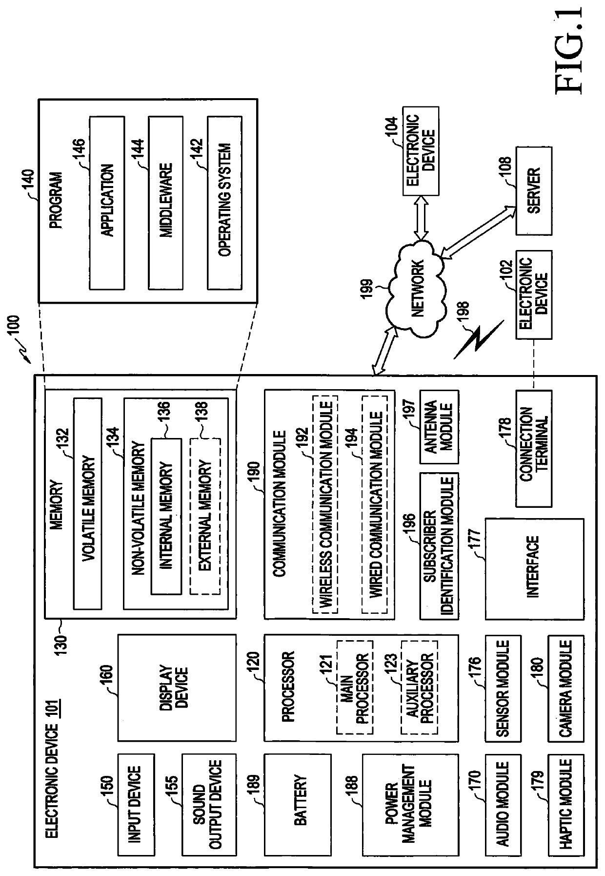
[0041]FIG. 1 is a block diagram illustrating an electronic device 101 in a network environment 100 according to various embodiments. Referring to FIG. 1, the electronic device 101 in the network environment 100 may communicate with an electronic device 102 via a first network 198 (e.g., a short-range wireless communication network), or an electronic device 104 or a server 108 via a second network 199 (e.g., a long-range wireless communication network). According to an embodiment, the electronic device 101 may communicate with the electronic device 104 via the server 108. According to an embodiment, the electronic device 101 may include a processor 120, memory 130, an input device 150, a sound output device 155, a display device 160, an audio module 170, a sensor module 176, an interface 177, a haptic module 179, a camera module 180, a power management. module 188, a battery 189, a communication module 190, a subscriber identification module (SIM) 196, or an antenna module 197. In so...


PUM

PropertyMeasurementUnit
wavelengthaaaaaaaaaa
wavelength bandaaaaaaaaaa

Abstract

Various embodiments of the present document relate to a display and, particularly, relate to a display including infrared elements, and an electronic device including the same. The display according to various embodiments of the present document includes a substrate; a first element for outputting light of a first visible light band and a second element for outputting light of an infrared band, the elements being formed on the substrate; and a third element for outputting light of a second visible light band, wherein at least a portion of the third element is arranged to overlaps the second element.

Description

CROSS-REFERENCE TO RELATED APPLICATION(S)[0001]This application is a National Phase Entry of PCT International Application No. PCT / KR2019 / 000899, which was filed on Jan. 22, 2019 and claims priority to Korean Patent Application No. 10-2018-0008359, which was filed on Jan. 23, 2018, the contents of each of which are incorporated herein by reference.BACKGROUND1. Field[0002]Various embodiments disclosed in the document relate to a display and, specifically, relate to a display including infrared elements and an electronic device including the same.2. Description of the Related Art[0003]In general, electronic devices denote devices for executing specific functions according to installed programs, such as electronic organizers, portable multimedia players, mobile communication terminals, tablet PCs, video / audio devices, desktop / laptop computers, vehicle navigation devices, or the like, as well as home appliances. For example, these electronic devices may output stored information as audi...

Claims


Application Information

Patent Timeline
Patent Type & Authority Applications(United States)
IPC IPC(8): H01L27/146H01L27/32G06K9/00G06F3/041
CPCH01L27/14652G06F3/0412G06K9/0004H01L27/323H04M1/026H04M1/0266H04M2250/12H10K59/32H10K59/351H10K59/65H10K50/19H04M1/724H04M2201/34H04M2201/38G06V40/12G06V40/1318H10K59/40
Inventor HEO, CHANGRYONGKIM, MINUKPRUSHINSKIY, VALERIYCHO, CHIHYUN
Owner SAMSUNG ELECTRONICS CO LTD
Why Eureka
Try Eureka