Thin light-emitting diode package

a light-emitting diode and package technology, applied in the field of compact light-emitting diode packages, can solve the problems of reducing the yield rate of thin films and cracks, and achieve the effects of reducing yield rate, stress hardly being concentrated, and improving the yield rate of light-emitting diodes

Active Publication Date: 2021-02-18
EPISTAR CORP
View PDF3 Cites 0 Cited by
  • Summary
  • Abstract
  • Description
  • Claims
  • Application Information

AI Technical Summary

Benefits of technology

[0009]Since the distance between the bumps of the light-emitting diode package is small, which results in a stress hardly being concentrated at the space between the bumps, as a result, a crack is difficultly caused by the stress to the light-emitting diode package. While being manufactured, the yield rate of the light-emitting diode package is improved since there is almost no crack to reduce the yield rate. Still, the lateral surface / edge of the first part of one bump is formed together with the adjacent lateral surface of the first part of the other bump in a period-repeating wriggle shape or an irregular wriggle shape, so that the structural strength between the bumps and the covering part is enhanced.

Problems solved by technology

However, the distance between the bumps of the thin film LED package is large, which results in a stress being concentrated at the space between one bump to the other one, therefore, a crack is caused by the stress to the thin film LED package.
The crack also reduces the yield rate of thin film LED package during the manufacture.

Method used


Image

  • Thin light-emitting diode package
  • Thin light-emitting diode package
  • Thin light-emitting diode package

Examples


Embodiment Construction

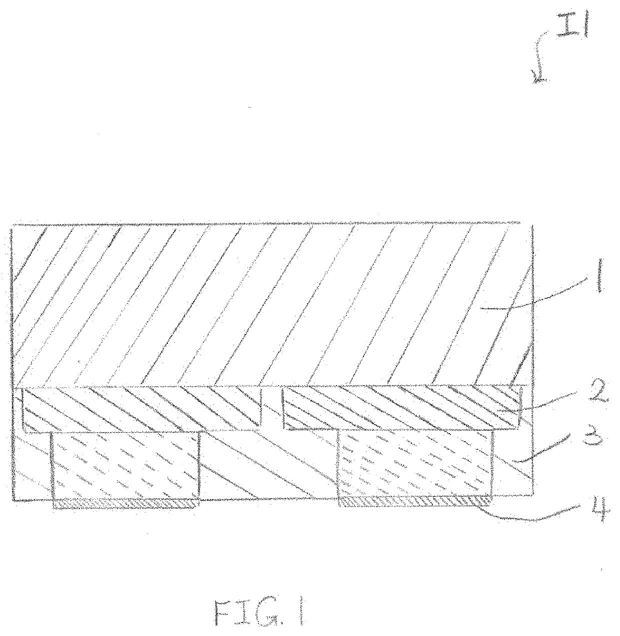
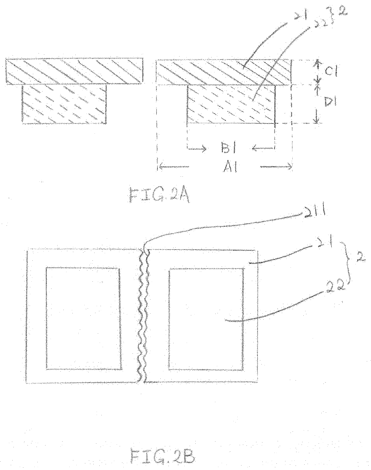
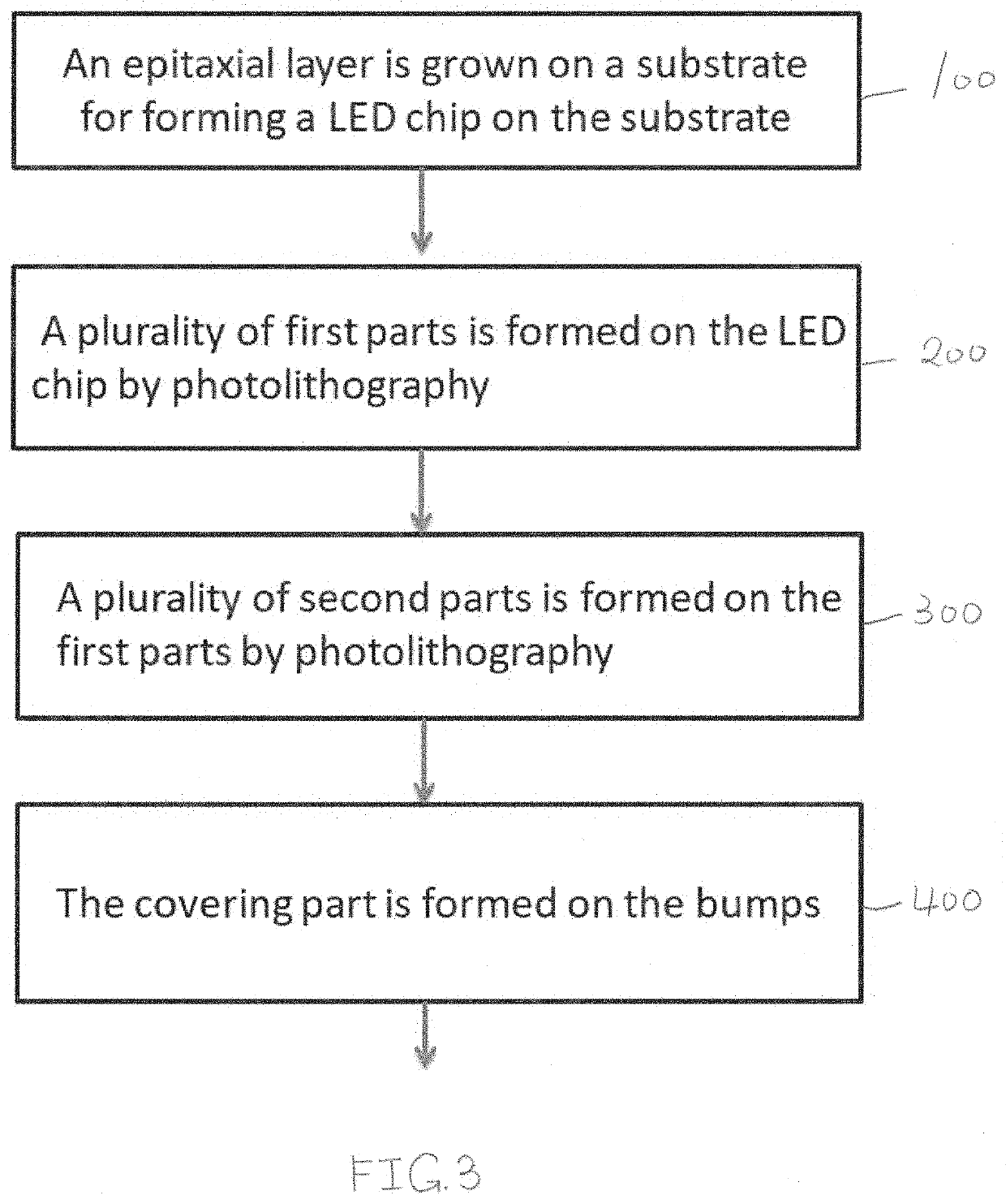
[0034]The present disclosure discloses a light-emitting diode package. The drawings referred in the following are not made according to the actual related sizes, and the function of these drawings is only for illustrating characteristics related to the present disclosure.

[0035]FIG. 1 is a cross sectional view of the light-emitting diode package according to a first preferred embodiment of the present disclosure. The light-emitting diode package 11 includes an LED chip 1, a plurality of bumps 2, a covering part 3, and a plurality of plates 4. The LED chip 1 is placed on the bumps 2. The bumps 2 are covered by the covering part 3. Each of the bumps 2 is connected to respective plates 4. The material of the bumps 2 is, for example, Cu, Ni, Cr, Sn or Ag. The foregoing material of the bumps 2 is an example. The material of the covering part 3 is, for example, epoxy or silicone. The foregoing material of the covering part 3 is an example. The material of the plates 4 is, for example, NiAu...


PUM

PropertyMeasurementUnit
widthaaaaaaaaaa
widthaaaaaaaaaa
vertical heightaaaaaaaaaa

Abstract

The light-emitting diode package includes a plurality of bumps being a couple corresponding to each other. Each of the bumps has a first part and a second part placed under the first part, and a gap is formed between the bumps in a period-repeating wriggle shape or an irregular wriggle shape. Accordingly, the distance between the bumps of the light-emitting diode package is small, which results in a less stress being concentrated at the space between the bumps, as a result, a crack is difficultly caused by the stress to the light-emitting diode package. In other words, the structural strength between the bumps and the covering part is enhanced. Still, while being manufactured, the yield rate of the light-emitting diode package is also improved since there is almost no crack to reduce the yield rate.

Description

BACKGROUND OF THE DISCLOSUREField of the Disclosure[0001]The present disclosure is related to a light-emitting diode package having a bare chip without a growth substrate, and more particularly to a compact light-emitting diode package with high yield rate.Description of the Prior Art[0002]The substrate of traditional light-emitting diode (LED) package has its characteristics, such as low heat dissipating rate, large emitting angle and so on. Therefore, new type LED package is developed as required, which is sometimes called thin film LED package. Since having no growth substrate, the thin film LED package is thin and has smaller emitting angle than the traditional type. However, the distance between the bumps of the thin film LED package is large, which results in a stress being concentrated at the space between one bump to the other one, therefore, a crack is caused by the stress to the thin film LED package. The crack also reduces the yield rate of thin film LED package during th...

Claims


Application Information

Patent Timeline
Patent Type & Authority Applications(United States)
IPC IPC(8): H01L33/20H01L33/38
CPCH01L33/20H01L33/38
Inventor SU, YING-YONGLIU, HSIN-MAOHU, WEI-SHANCHENG, CHING-TAI
Owner EPISTAR CORP
Why Eureka
Try Eureka