Device and method for simultaneously inspecting defects of surface and subsurface of optical element

a technology of optical elements and devices, applied in the direction of color/spectral properties measurement, instrumentation, and solid analysis using sonic/ultrasonic/infrasonic waves, can solve the problems of incomplete inspection and evaluation technologies for subsurface defects, decrease in material mechanical properties, and macroscopic damage of optical elements, so as to improve the sensitivity of scattering inspection and effectively identify the defect position

Active Publication Date: 2021-02-25
ZHEJIANG UNIV
View PDF0 Cites 2 Cited by
  • Summary
  • Abstract
  • Description
  • Claims
  • Application Information

AI Technical Summary

Benefits of technology

[0041]Firstly, the present invention can simultaneously inspect the defects of the surface and the subsurface of the optical element and provide the intuitive defect distribution image through the scanning way.
[0042]Secondly, based on the acoustic surface wave excited by the exciting laser, the present invention modulates the scattering effects of the surface and the subsurface of the optical element, which improves the sensitivity of the scattering inspection and can effectively identify the defect positions.

Problems solved by technology

The surface / subsurface damages introduced during the manufacturing process influence the damage sensitivity of the optical elements from three aspects respectively of light field strengthening caused by the interference, enhanced laser absorption ability of the optical material by the cracks and impurities, and decrease of the material mechanical property, further causing the macroscopic damages of the optical elements.
However, the inspection and evaluation technologies for the subsurface defects are still not complete.
The minor damages hidden 1-100 μm below the surface directly decrease the property and service life of the optical material and cause the irreversible damages to the elements.
However, the current technologies have deficiencies as follows.
(1) The current inspection methods are only the static observation of the defect positions within the limited time, whose sensitivity and precision on the subsurface defects are generally poor.
(2) The current technologies adopt the single scattered light collection and analysis means to analyze the scattering effects of different defects, which fails to evaluate the dynamic changes of the defects in motion.
However, at present, there are few effective nondestructive inspection methods.

Method used


Image

  • Device and method for simultaneously inspecting defects of surface and subsurface of optical element
  • Device and method for simultaneously inspecting defects of surface and subsurface of optical element
  • Device and method for simultaneously inspecting defects of surface and subsurface of optical element

Examples


Embodiment Construction

[0047]The present invention is further described in detail with the accompanying drawings and the preferred embodiment.

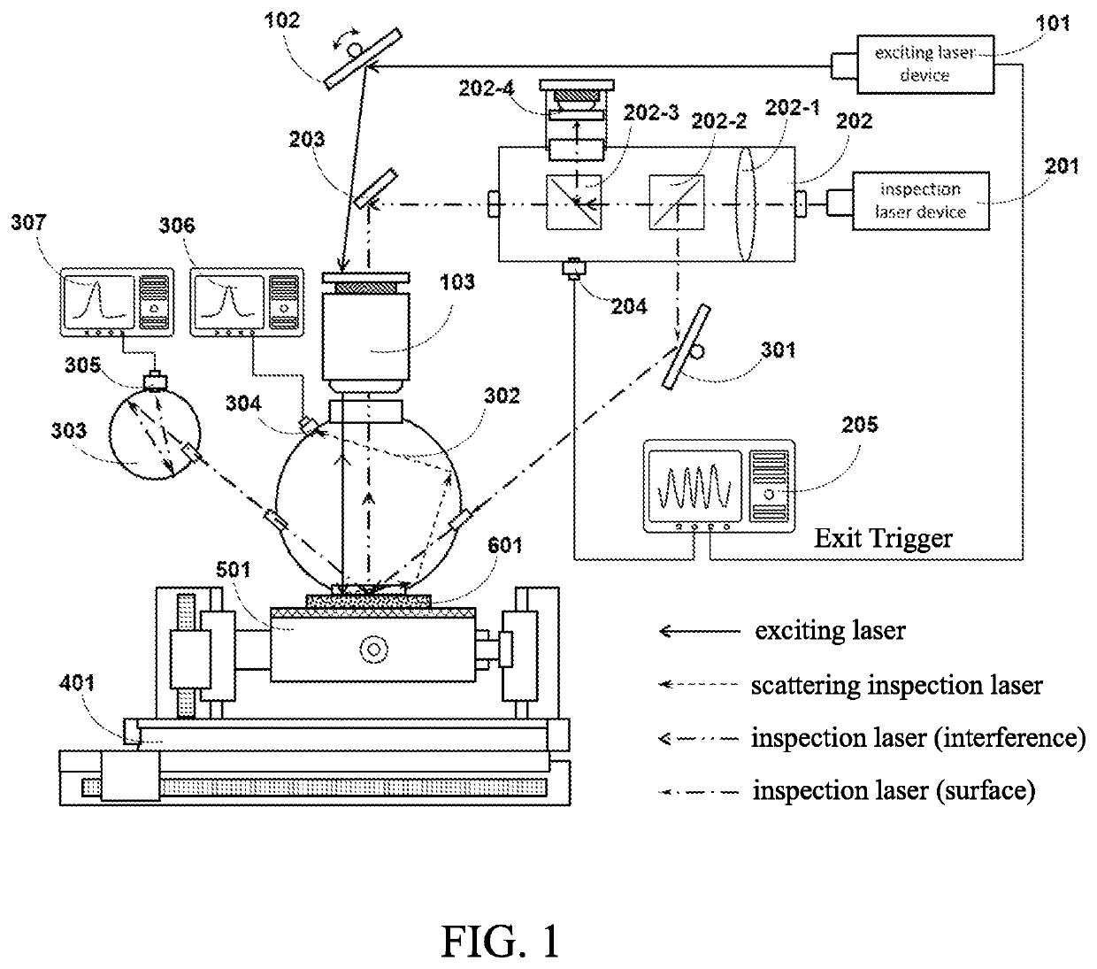
[0048]According to the preferred embodiment of the present invention, a device and a method for simultaneously inspecting defects of a surface and a subsurface of an optical element are provided, which can be applied in quality inspection of optical elements, especially in finished product inspection of ultra-precise optical elements having strict requirements on subsurface defects.

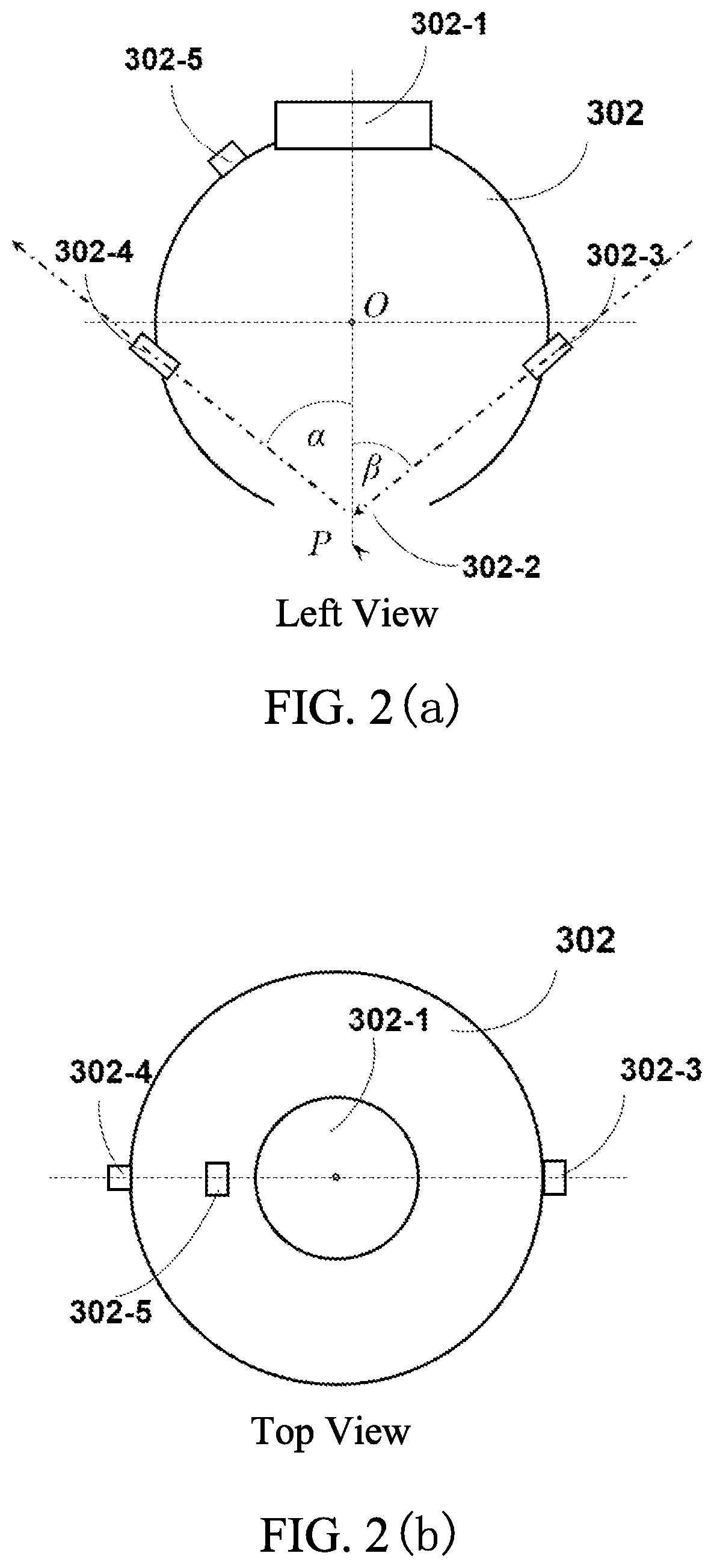
[0049]As shown in FIG. 1, the device for simultaneously inspecting the defects of the surface and the subsurface of the optical element comprises a laser excitation device, a laser interference inspection device, a laser scattering inspection device, a motion platform 401 and a sample table 501.

[0050]According to the preferred embodiment of the present invention, the laser excitation device and the laser interference inspection device adopt lasers of different wavelengths; the laser inter...


PUM

PropertyMeasurementUnit
wavelengthaaaaaaaaaa

Abstract

A device and a method for simultaneously inspecting defects of a surface and a subsurface of an optical element are provided. Combined with laser-induced ultrasound and laser scattering inspection technologies, through generating acoustic sound waves on the surface and the subsurface of the optical element to be tested by lasers, a static light scattering effect of subsurface defects under modulation of the acoustic sound wave is observed and analyzed; through analyzing amplitude and phase changes of scattered light intensity and reflected light intensity, inspection for the defects of the surface and the subsurface of the optical element is realized. The present invention can be applied in quality inspection of precise optical elements, especially in finished product inspection of ultra-precise optical elements having strict requirements on the subsurface defects.

Description

BACKGROUND OF THE PRESENT INVENTIONField of Invention[0001]The present invention relates to a nondestructive inspection technology, and more particularly to a device and a method for simultaneously inspecting defects of a surface and a subsurface of an optical element. The present invention can be applied in quality inspection of precise optical elements, especially in finished product inspection of ultra-precise optical elements having strict requirements on subsurface defects.Description of Related Arts[0002]The technological developments of the fields such as high-precision optical system, high-performance laser weapons and inertial confinement laser fusion system around the world raise the unprecedented strict requirements on the damage resistance ability of the optical elements. The surface / subsurface damages introduced during the manufacturing process influence the damage sensitivity of the optical elements from three aspects respectively of light field strengthening caused by...

Claims


Application Information

Patent Timeline
Patent Type & Authority Applications(United States)
IPC IPC(8): G01N21/88G01N21/17G01N21/49
CPCG01N21/8806G01N21/1702G01N2201/06113G01N2021/1706G01N21/49G01N21/19G01N21/27G01N21/45G01N21/47G01N21/55G01N21/958G01N29/07G01N29/2418G01N2021/4702G01N2021/4735G01N2201/065G01N2291/011G01N2291/0423
Inventor SUN, ANYULI, ZHIHONGJU, BINGFENGWANG, CHUANYONGYANG, XIAOYUSUN, ZEQINGDU, HUILIN
Owner ZHEJIANG UNIV
Why Eureka
Try Eureka