High frequency switch and antenna device
a high-frequency switch and antenna technology, applied in the direction of antennas, multiple-port active networks, transmission, etc., can solve the problems of noise generation, the level of a high-frequency signal passing through the switch is reduced, etc., and achieves low loss and high speed
- Summary
- Abstract
- Description
- Claims
- Application Information
AI Technical Summary
Benefits of technology
Problems solved by technology
Method used
Image

Examples
first embodiment
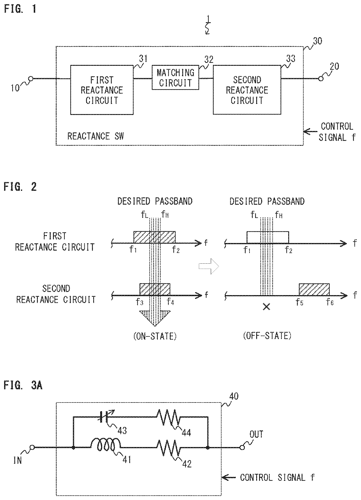
[0027]FIG. 1 is a configuration diagram of a high-frequency switch according to a first embodiment. The high-frequency switch 1 includes an input interface 10, an output interface 20, and a reactance SW (or a reactance switch; hereinafter the same) 30 inserted between them, all of which are formed on, for example, an insulating substrate which is rectangular or substantially rectangular in shape and is less than or equal to about 10 mm square in size.
[0028]The input interface 10 is a signal input terminal with a grounding end and a signal end, for example, and receives a high-frequency signal in the 29 GHz band at the signal end. The output interface 20 is a signal output terminal with a grounding end and a signal end, for example. The high-frequency switch 1 forms a first state in which a high-frequency signal input to the input interface 10 is output from the output interface 20, and a second state in which a high-frequency signal input to the input interface 10 is reflected by th...
second embodiment
[0057]The high-frequency switch 1 of the first embodiment is an example in which the switch is suited to be operated as an SPST (Single Pole, Single Throw) switch. However, the high-frequency switch of the present invention may also be implemented as an SPnT switch (n is a natural number more than or equal to 2).
[0058]FIG. 7 is a configuration diagram of a high-frequency switch 2 according to a second embodiment. The high-frequency switch 2 includes one input interface 10, a reactance SW 70, and three (three sets of) output interfaces 21, 22, and 23.
[0059]The reactance SW 70 includes a first reactance circuit 71 connected to the input interface 10; a branch circuit 72 which branches a high-frequency signal having passed through the first reactance circuit 71 into three transmission paths; and matching circuits 731, 732, and 733 and second reactance circuits 741, 742, and 743 provided between the branched transmission paths and the output interfaces 21, 22, and 23, respectively. Thes...
third embodiment
[0067]Although the second embodiment illustrates an example in which one input interface and a plurality of output interfaces are provided, it is also possible to provide a plurality of input interfaces and one output interface. A third embodiment will describe an example of such a high-frequency switch.
[0068]FIG. 9 is a configuration diagram of a high-frequency switch according to the third embodiment. A high-frequency switch 3 of the third embodiment is obtained by reversing the input-output relationship of the high-frequency switch 2 of the second embodiment illustrated in FIG. 7 and using the branch circuit 72 of the reactance SW 70 of the second embodiment as a combining circuit 82. That is, the high-frequency switch 3 includes three input interfaces 11, 12, and 13. These correspond to the output interfaces 21, 22, and 23 of the high-frequency switch 2 of the second embodiment. In addition, the high-frequency switch 3 includes an output interface 20. This corresponds to the inp...
PUM
 Abstract
Description
Claims
Application Information
 - R&D Engineer
- R&D Manager
- IP Professional
- Industry Leading Data Capabilities
- Powerful AI technology
- Patent DNA Extraction
Browse by: Latest US Patents, China's latest patents, Technical Efficacy Thesaurus, Application Domain, Technology Topic.
© 2024 PatSnap. All rights reserved.Legal|Privacy policy|Modern Slavery Act Transparency Statement|Sitemap