Anomaly Detection and Remedial Recommendation

Active Publication Date: 2021-03-04
IBM CORP
View PDF0 Cites 9 Cited by
  • Summary
  • Abstract
  • Description
  • Claims
  • Application Information

AI Technical Summary

Benefits of technology

[0005]The present invention provides anomaly detection and remedial recommendation techniques for improving the quality and yield of microelectronic products. In one aspect of the invention, a method for quality and yield improvement via anomaly detection is provided. The method includ

Problems solved by technology

Investing time, energy and resources into chips that ultimately need to be re-worked or

Method used


Image

  • Anomaly Detection and Remedial Recommendation
  • Anomaly Detection and Remedial Recommendation
  • Anomaly Detection and Remedial Recommendation

Examples


Embodiment Construction

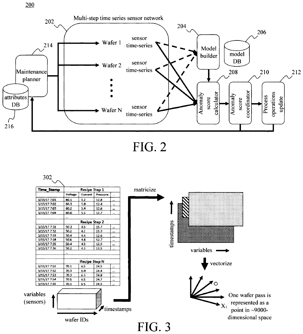
[0024]As highlighted above, the overall quality and yield of microelectronic products depends on the quality and yield of individual unit processes and the successful integration of a multitude of unit processes performed using a multitude of processing steps at various different fabrication stages. Provided herein are techniques for improving the quality and yield of individual unit processes or aggregations thereof to improve the overall quality and yield of the resulting microelectronic products.

[0025]As will be described in detail below, the unit process quality is inferred using metrics such as tool sensor time series measurements (which reflect tool condition and wafer recipes), incoming (i.e., partially completed) product characteristics, and other data. For instance, according to an exemplary embodiment, the present techniques employ a predictive model of semiconductor manufacturing using toolset-related data, wafer data, and auxiliary data (i.e., all other data used to buil...


PUM


Abstract

Anomaly detection and remedial recommendation techniques for improving the quality and yield of microelectronic products are provided. In one aspect, a method for quality and yield improvement via anomaly detection includes: collecting time series sensor data during individual steps of a semiconductor manufacturing process; calculating anomaly scores for each of the individual steps using a predictive model; and implementing changes to the semiconductor manufacturing process based on the anomaly scores. A system for quality and yield improvement via anomaly detection is also provided.

Description

FIELD OF THE INVENTION[0001]The present invention relates to microelectronic processing, and more particularly, to anomaly detection and remedial recommendation techniques for improving the quality and yield of microelectronic products.BACKGROUND OF THE INVENTION[0002]The overall quality and yield of microelectronic products depends on the quality and yield of individual unit processes and the successful integration of many (e.g., hundreds) of unit processes. For instance, a typical semiconductor integrated circuit fabrication process involves the coordination of many different steps performed in stages to produce end-product chips. The input to each stage involves a variety of often variable components (e.g., incoming wafer variability, masking level variability, etc.), each of which can introduce anomalies that affect the viability of the end-product chips, i.e., whether the end-product chips are within specifications, or need to be re-worked or scrapped.[0003]Investing time, ener...

Claims


Application Information

Patent Timeline
IPC IPC(8): H01L21/66G01R31/26G06N7/00G06N20/00
CPCH01L22/14G06N20/00G06N7/005G01R31/2601G05B19/41875H01L22/20G05B2219/32194G05B2219/32208G05B2219/32179G05B2219/37224G06N3/088G06N7/01G06N3/044G06N3/045
Inventor PHAN, DZUNGBASEMAN, ROBERTNGUYEN, NAM H.TIPU, FATEHMURALIDHAR, RAMACHANDRAN
Owner IBM CORP
Why Eureka
Try Eureka