Array substrate and OLED display device
- Summary
- Abstract
- Description
- Claims
- Application Information
AI Technical Summary
Benefits of technology
Problems solved by technology
Method used
Image


Examples
embodiment 1
[0078]As shown in FIG. 2B, the pixel structure of the array substrate of the present disclosure is that each column of the sub-pixels 201 corresponds to one of the data lines 202 and one of the power supply signal lines 203, and the data lines 202 and the power supply signal lines 203 at least partially overlap. In this way, area occupied by vertical lines in the pixel structure is reduced. It can be known from FIG. 2B and FIG. 1, the reduced area between the power supply signal lines 203 and the data lines 202 of the pixel structure in the embodiment makes aperture ratio of the pixel increase.
[0079]The sub-pixels in the embodiment is R, G, or B, but it is not limited the three kinds of the sub-pixels 201 in other embodiments, and the arrangement of the sub-pixels 201 is not limited.
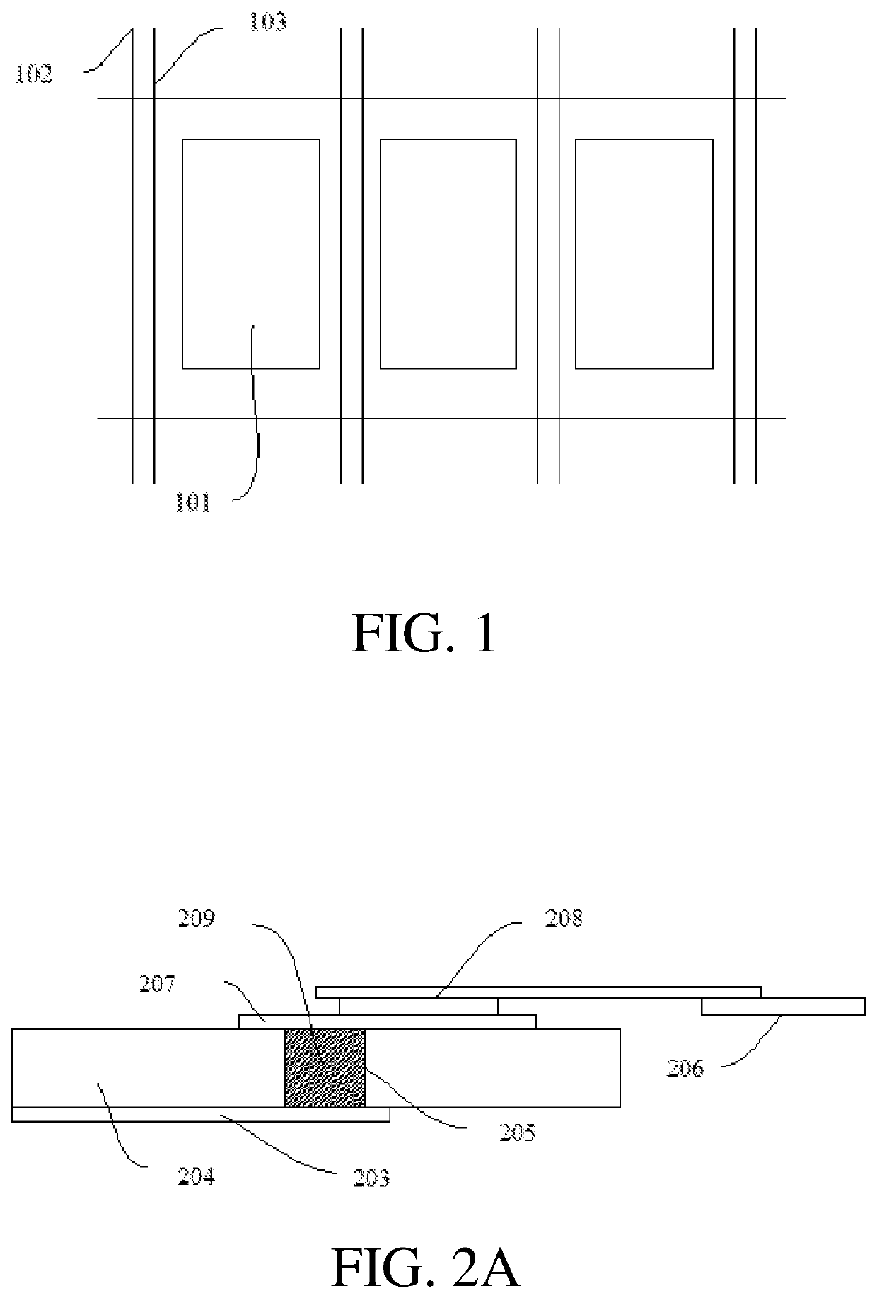
[0080]FIG. 2C is a schematic cross-sectional structural diagram of area A-A′ in FIG. 2B. In the figure, from the top to the bottom are respectively the data lines 202, a gate insulating layer 210, scann...
embodiment 2
[0093]FIG. 3C is a pixel equivalent circuit diagram of an array substrate of the present disclosure. One sub-pixel of the array substrate comprises a first thin film transistor T1, a second thin film transistor T2, a third thin film transistor T3, scanning lines Gate, cathode signal lines VSS, the data lines Data, the power supply signal lines VDD, the compensation signal lines Vc, and a storage capacitor Clc; an adjacent sub-pixel thereof comprises a fourth thin film transistor T4, a fifth thin film transistor T5, a sixth thin film transistor T6, the scanning lines Gate, the cathode signal lines VSS, the data lines Data, the power supply signal lines VDD, the compensation signal lines Vc, and the storage capacitor Clc. Wherein a gate electrode of the first thin film transistor T1 is electrically connected to the scanning lines Gate, and a source electrode of the first thin film transistor T1 is electrically connected to an N-th level data line Data(n); wherein a gate electrode of ...
PUM
 Abstract
Description
Claims
Application Information