Image pickup apparatus, endoscope, and manufacturing method of image pickup apparatus
- Summary
- Abstract
- Description
- Claims
- Application Information
AI Technical Summary
Benefits of technology
Problems solved by technology
Method used
Image

Examples
first embodiment
Modifications of First Embodiment
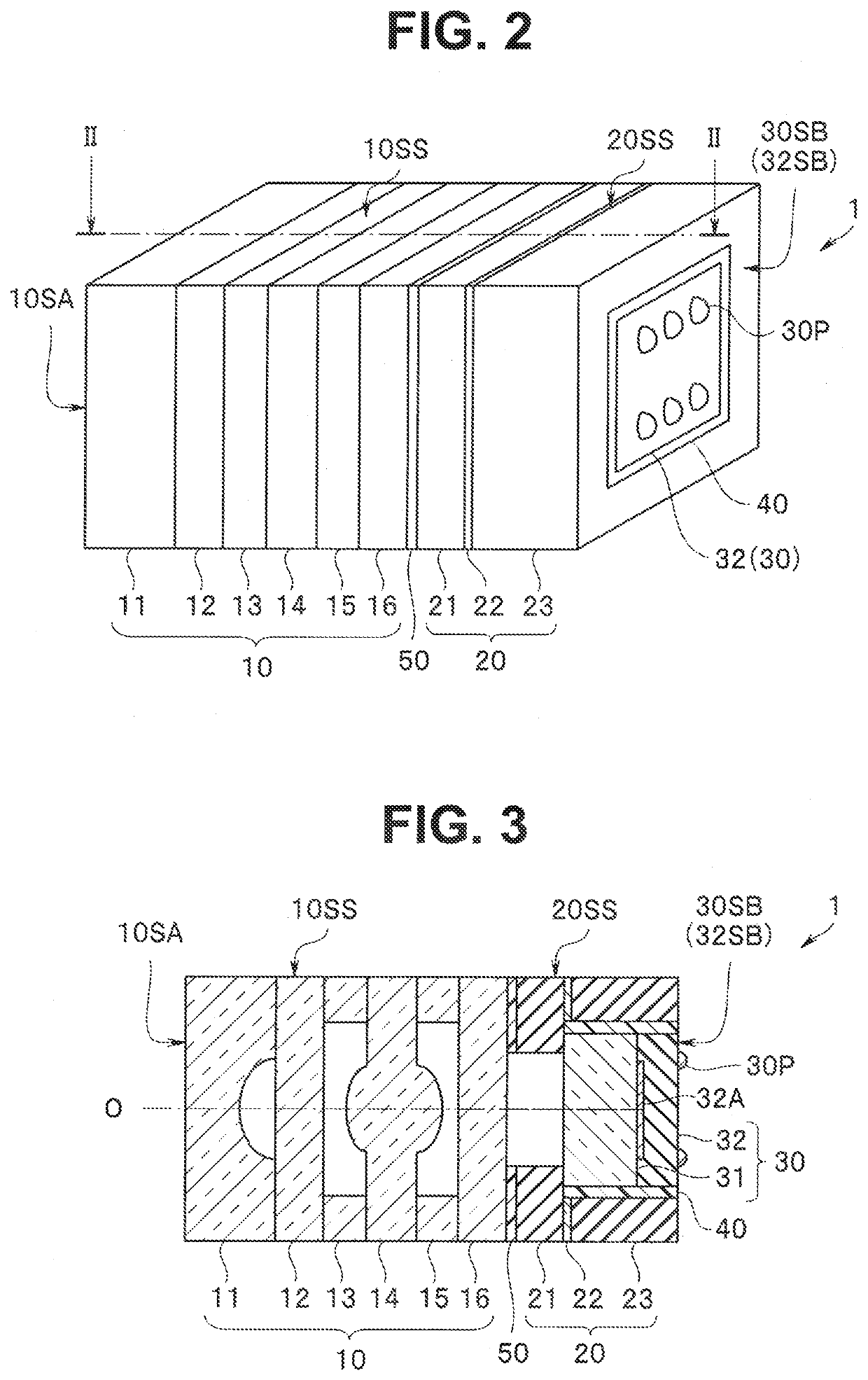
[0090]Various modifications can be made for the holding portion 20.
[0091]In the holding portion 20 according to the first modification illustrated in FIG. 14, a notch (recession) N23 is provided at an outer peripheral edge of an opening of the second through-hole H23 in the third main surface 23SA of the frame 23. The notch N23 that is a cut portion is an overetched region formed when the second through-hole H23 is formed.
[0092]The notch N23 can effectively prevent the adhesive 40 from entering the abutting surface between the front surface 30SA and the second main surface 21SB when the uncured adhesive 40 is poured between the image pickup side surface 30SS and the wall surface 20HSS of the second through-hole H23. In other words, since the excessive adhesive 40 is accommodated in the notch N23 and does not spread on the abutting surface.
[0093]In the holding portion 20 according to the second modification illustrated in FIG. 15, a notch N20 that is ...
second embodiment
[0097]Note that since image pickup apparatuses 1A to 1C according to the following embodiments are similar to the image pickup apparatus 1 and have similar advantages, the same reference signs will be applied to components with the same functions, and description will be omitted.
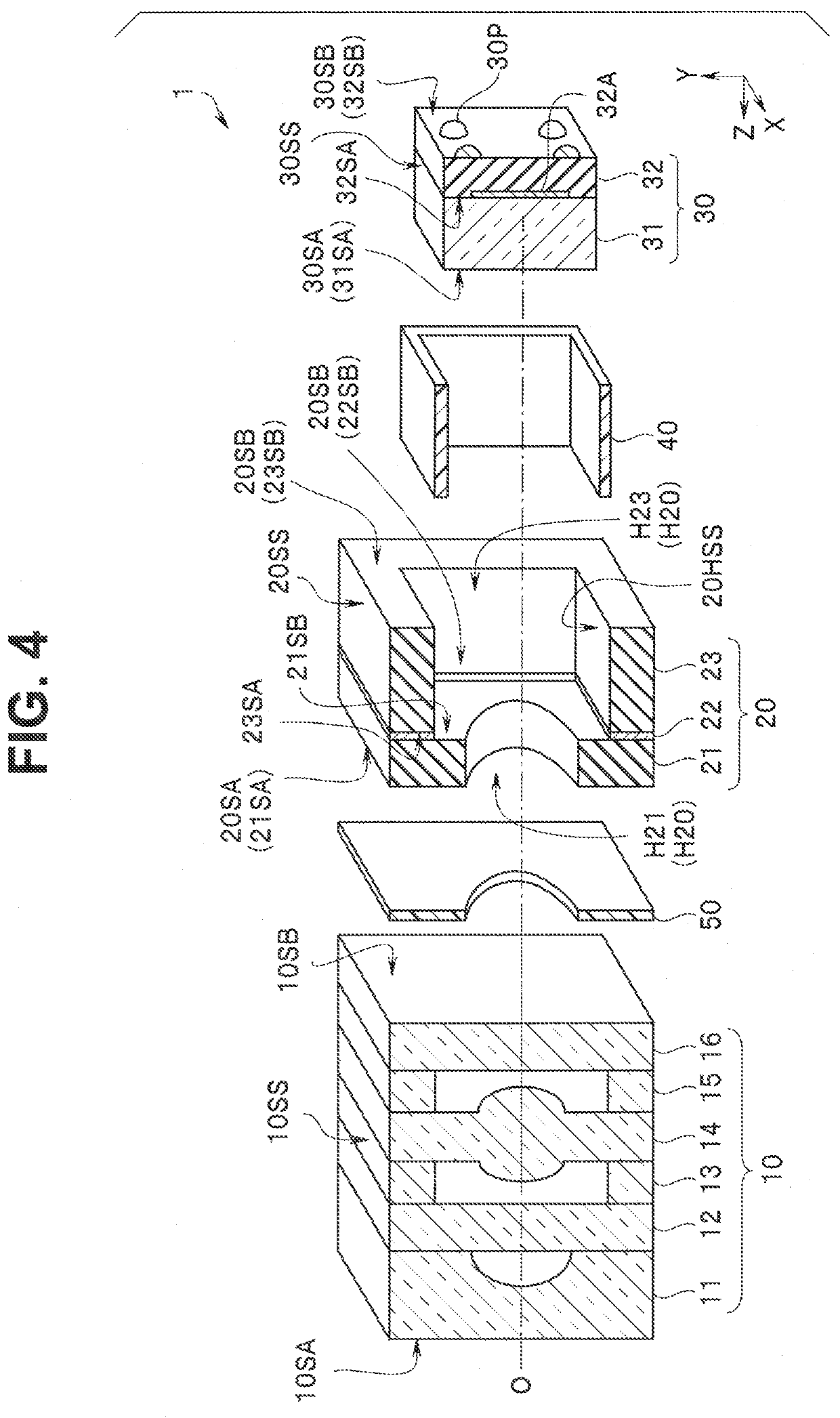
[0098]The image pickup apparatus 1A illustrated in FIG. 16 includes no silicon oxide layer between a spacer 21 and a frame 23 of a holding portion 20A.
[0099]In the image pickup apparatus 1A, a holding wafer 20W is produced through bonding of two silicon wafers. For example, a first silicon wafer in which a first through-hole H21 is formed and a second silicon wafer in which a second through-hole H23 is formed are bonded directly to each other, thereby producing the holding wafer 20W. In other words, the silicon oxide layer is not an essential component of the holding wafer 20W (holding portion 20).
[0100]In other words, it is only necessary for the holding portion to include the spacer 21 and the frame 23.
third embodiment
[0101]The image pickup apparatus 1B illustrated in FIG. 17 further includes a laminated semiconductor 39 bonded to a back surface 30SB of an image pickup unit 30. The laminated semiconductor 39 in which a plurality of semiconductor devices 33 to 35 are laminated is disposed in a second through-hole H23.
[0102]The semiconductor devices 33 to 35 perform primary processing on image pickup signals outputted from an image pickup device 32 and perform processing on control signals for controlling the image pickup device 32. For example, the semiconductor devices 33 to 35 include an AD conversion circuit, a memory, a transmission output circuit, a filter circuit, a capacitor, a resistor, or an inductor. The number of semiconductor devices included in the laminated semiconductor 39 is, for example, equal to or greater than one and equal to or less than ten. Each of the plurality of semiconductor devices 33 to 35 is electrically connected via a penetrating wiring (not illustrated).
[0103]In a ...
PUM
 Abstract
Description
Claims
Application Information
 - R&D Engineer
- R&D Manager
- IP Professional
- Industry Leading Data Capabilities
- Powerful AI technology
- Patent DNA Extraction
Browse by: Latest US Patents, China's latest patents, Technical Efficacy Thesaurus, Application Domain, Technology Topic.
© 2024 PatSnap. All rights reserved.Legal|Privacy policy|Modern Slavery Act Transparency Statement|Sitemap