


Quick Research
Generate reliable direction feasibility study reports for your R&D in just a few steps.

Technical Q&A
Discover and master advanced knowledge NOW. Basics, ideas, possibilities, all at once.

Find Solutions
As an expert in R&D theories, this can generate solutions to your technical problems instantly.

Evaluate Feasibility
Analyze your overall solution with one click, know your potential R&D risks in advance.

Monitor Landscape
Get weekly tech updates, stay abreast of the latest tech innovations and key insights.
Semiconductor device
a semiconductor element and semiconductor technology, applied in vehicle headlamps, transportation and packaging, lighting and heating apparatus, etc., can solve the problems of reducing long-term reliability, damage to the electrodes of semiconductor elements and the mounting substrate, etc., and achieve the effect of reducing mounting damag
- Summary
- Abstract
- Description
- Claims
- Application Information
AI Technical Summary
Benefits of technology
Problems solved by technology
Method used
Image

Examples
embodiment 1
[Semiconductor Device]
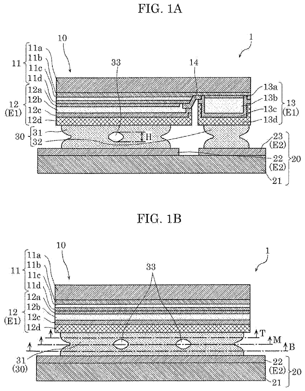
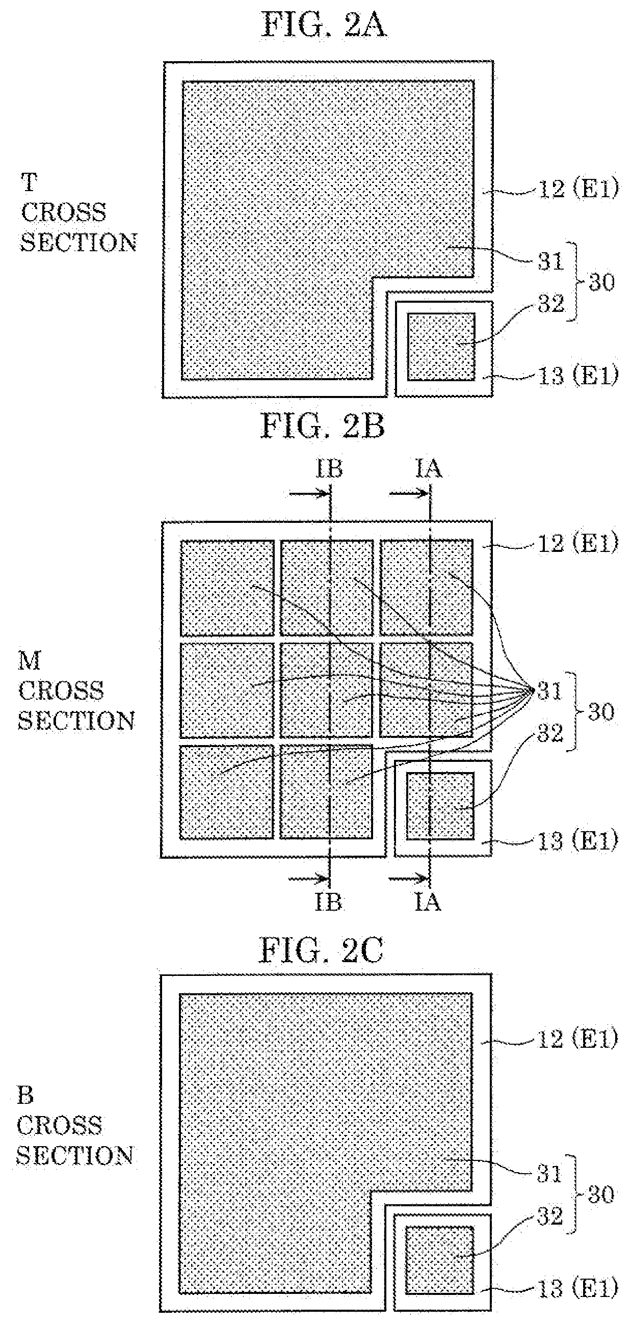
[0074]First, the configuration of semiconductor device 1 according to Embodiment 1 will be described with reference to FIG. 1A, FIG. 1B, and FIG. 2A to FIG. 2C. FIG. 1A and FIG. 1B are cross-sectional views of semiconductor device 1 according to Embodiment 1. FIG. 2A is a cross-sectional view of semiconductor device 1 in a T cross section obtained when cut along dashed line T in FIG. 1B. FIG. 2B is a cross-sectional view of semiconductor device 1 in an M cross section obtained when cut along dashed line M in FIG. 1B. FIG. 2C is a cross-sectional view of semiconductor device 1 in a B cross section obtained when cut along dashed line B in FIG. 1B. Note that FIG. 1A is a cross-sectional view taken along line IA-IA in FIG. 2B and FIG. 1B is a cross-sectional view taken along line IB-IB in FIG. 2B. In FIG. 2A to FIG. 2C, each of dashed lines T, M, B indicates a plane perpendicular to the thickness direction (height direction) of bonding metal layer 30. Dashed line M...
embodiment 2
Variation of Embodiment 2
[0231]Next, semiconductor device 2A according to a variation of Embodiment 2 will be described with reference to FIG. 19. FIG. 19 is a cross-sectional view illustrating semiconductor device 2A according to the variation of Embodiment 2. In FIG. 19, (a) is a cross-sectional view in which semiconductor element 10 has not yet been mounted on mounting substrate 20, and (b) is a cross-sectional view in which semiconductor element 10 has already been mounted on mounting substrate 20. In (a) and (b) in FIG. 19, the left diagram is a cross-sectional view taken along line X-X in the right diagram.
[0232]As illustrated in FIG. 19, in semiconductor device 2A according to the present variation, the outer side of first electrode E1 of semiconductor element 10 at least partially includes a curved section, as in semiconductor device 2 illustrated in FIG. 15.
[0233]Furthermore, in semiconductor device 2A according to the present variation, gap 33 inside bonding metal layer 30...
embodiment 3
[0235]Next, semiconductor device 3 according to Embodiment 3 will be described with reference to FIG. 20. FIG. 20 is a cross-sectional view illustrating the configurations of semiconductor device 3 according to Embodiment 3 before and after mounting. In FIG. 20, (a) is a cross-sectional view in which semiconductor element 10 has not yet been mounted on mounting substrate 20, and (b) is a cross-sectional view in which semiconductor element 10 has already been mounted on mounting substrate 20. In (a) and (b) in FIG. 20, the left diagram is a cross-sectional view taken along line X-X in the right diagram.
[0236]Semiconductor device 3 according to the present embodiment is different from semiconductor device 2 according to Embodiment 2 described above in that gap 33 inside bonding metal layer 30 has a different shape in a plan view. Specifically, in semiconductor device 3 according to the present embodiment, gap 33 is at least partially radial in shape in a plan view of bonding metal lay...
PUM
| Property | Measurement | Unit |
|---|---|---|
| distance | aaaaa | aaaaa |
| light-emission peak wavelength | aaaaa | aaaaa |
| thickness | aaaaa | aaaaa |
Abstract
Description
Claims
Application Information
 - R&D Engineer
- R&D Manager
- IP Professional
- Industry Leading Data Capabilities
- Powerful AI technology
- Patent DNA Extraction
Browse by: Latest US Patents, China's latest patents, Technical Efficacy Thesaurus, Application Domain, Technology Topic, Popular Technical Reports.
© 2024 PatSnap. All rights reserved.Legal|Privacy policy|Modern Slavery Act Transparency Statement|Sitemap|About US| Contact US: help@patsnap.com