

Method of enhancing copper electroplating
a technology of copper electroplating and copper electroplating plate, which is applied in the direction of basic electric elements, semiconductor devices, etc., can solve the problems of increasing manufacturing costs, complicated fill uniformity, and unsatisfactory conventional approaches to pattern formation and filling, so as to improve the quality of copper electroplating, increase or even decrease the plating rate, and improve the effect of copper morphology
- Summary
- Abstract
- Description
- Claims
- Application Information
AI Technical Summary
Benefits of technology
Problems solved by technology
Method used
Image

Examples
example 1
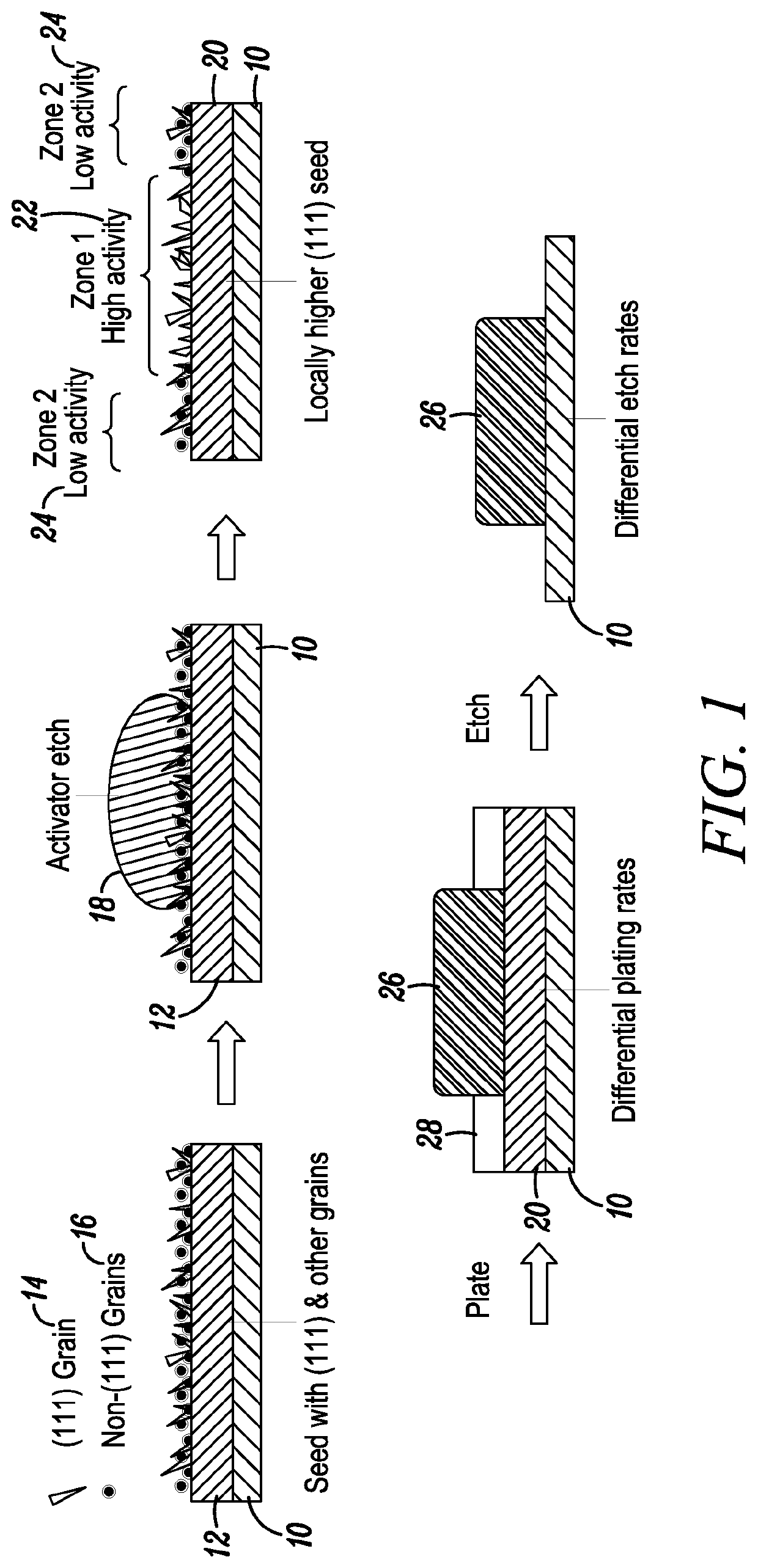
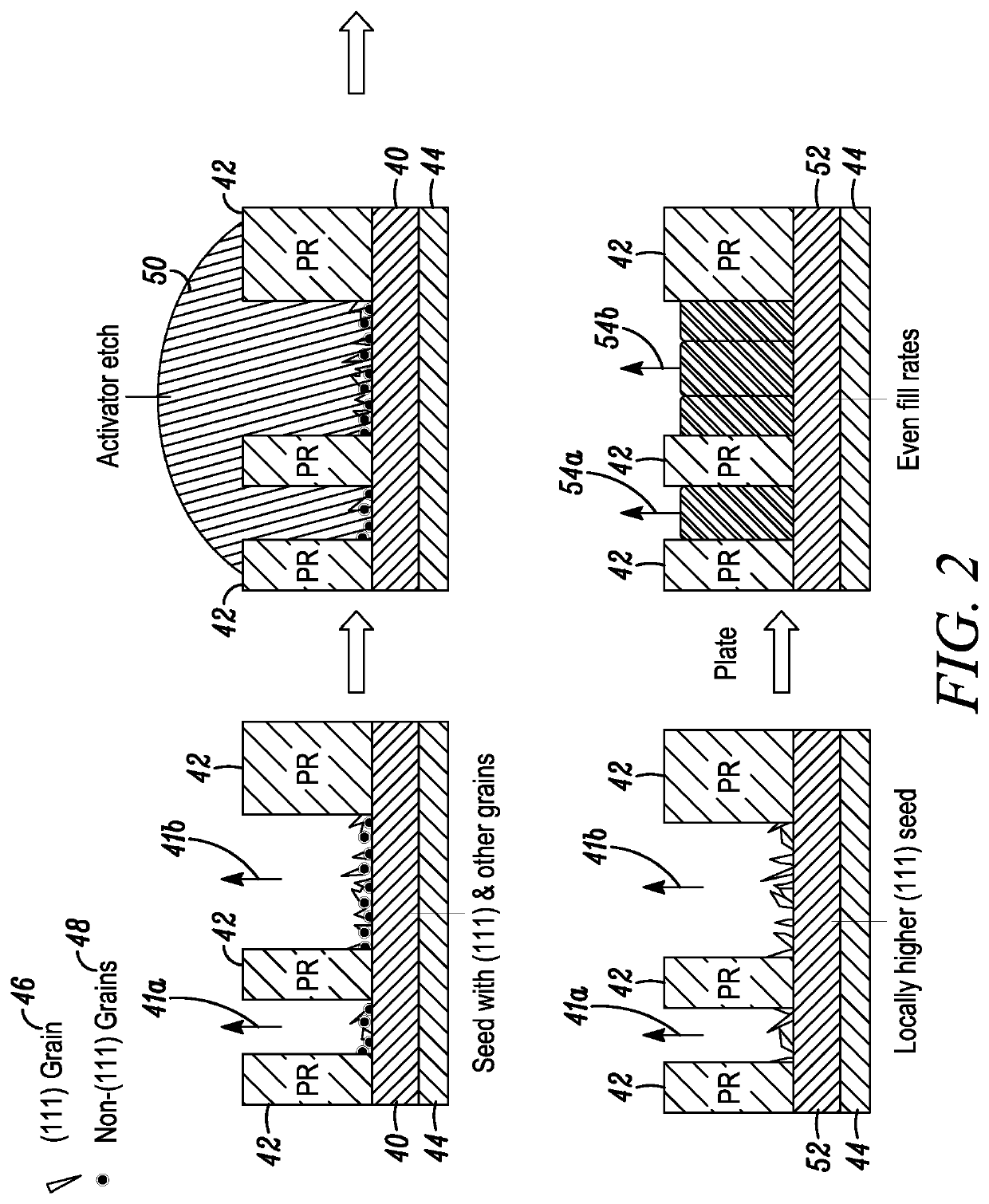
Modifying Exposed Copper Grain Orientation with TMAH
[0069]A plurality of silicon wafers with 180 nm thick copper seed layers obtained from WRS Materials (Vancouver, Wash.) were analyzed for their surface crystal plane (111) orientation using a Field Emission-SEM (FEI model Helios G3) coupled with EBSD detector (EDAX Inc., model Hikari Super and data was analyzed by OIM™ Analysis software). The prevalence of surface crystal plane (111) orientation grains on the copper seed was determined through the maximum in the IPF on the Z axis, represented by the Multiples of Uniform Density (MUD) value. The IPF data was collected on a 20 by 20 μm area of the seed surface using a 50 nm pixel pitch and a 50 Hz scan rate, which provided a hit rate higher than 50% in all samples. The higher the MUD value for the IPF on the Z axis, the more prevalent the crystal plane (111) orientation grains were on the surface of the copper seed layers. In addition, the copper seeds were analyzed via XRD spectrosc...
example 2
Electroplating Copper on TMAH Treated Copper Seed Layers
[0071]Three (3) areas of a 180 nm thick copper seed layers on 1 cm by 2 cm silicon wafers were treated with an aqueous 0.25M TMAH solution having a pH=14. The three separate treated areas had diameters of 3.5 mm, 4.5 mm and 6 mm, as determined with a Keyence optical profilometer. The diameters of the treated areas were varied by increasing the volume of the TMAH solution applied from 6 μL to 10 μL to 20 μL. The solution was left to act on the copper seed layers for 2 min at room temperature. The copper seed layers were then rinsed with DI water and dried under a stream of air. The copper seed layers were then electroplated with the copper electroplating bath of Table 1 below to a target field height of 6 μm plating at 2 ASD and a temperature of 25° C. The pH of the copper electroplating bath was <1.
TABLE 1ComponentAmountCopper (II) ions from copper sulfate50g / LpentahydrateSulfuric acid (98 wt %)100g / LChloride ions from HCl50ppm...
example 3
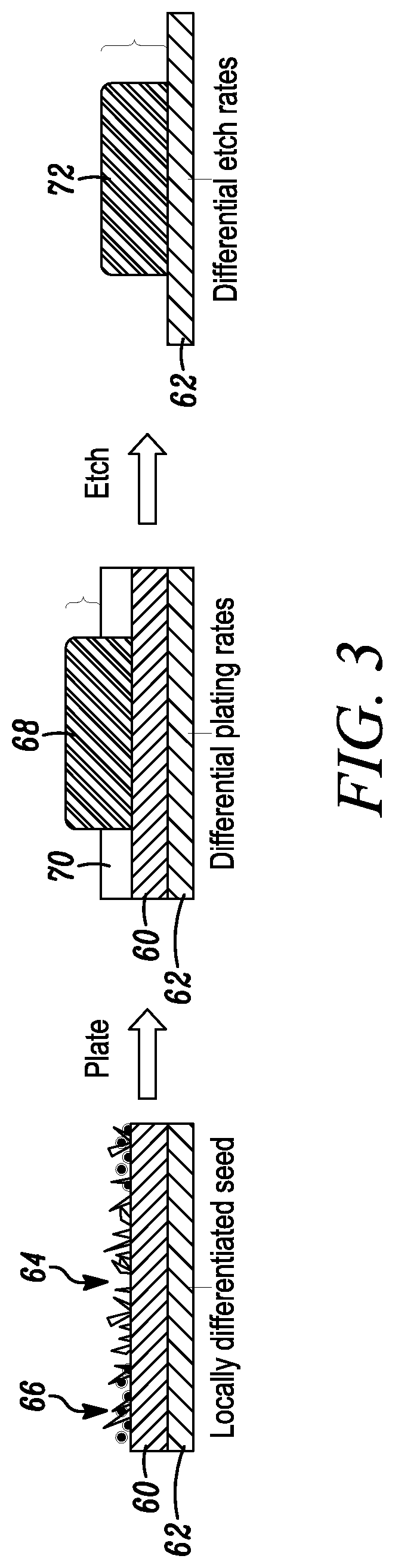
Electroplating Copper on TMAH Treated Copper Seed Layers and Etch Rate
[0073]10 μL aliquots of an aqueous 0.25M TMAH solution having a pH=14 with 4.2 mm diameters were applied onto a 180 nm thick copper seed layer 60 on a silicon wafer 62 as shown in FIG. 3. The solution acted on the copper seed layer surface for 2 min to increase the exposed copper grains having crystal plane (111) orientations 64 over the non-(111) copper grains and non-crystalline material 66. The copper seed layer was then rinsed with DI water and dried under a stream of air. The seed layer was then electroplated with the copper electroplating bath of Table 1 of Example 2 above to a target field height of 6 μm plating at 2 ASD. The height of the features that resulted from the treated areas versus the untreated field were then measured with a Keyence optical profilometer as in Example 2. The features retained the same 4.2 mm diameters as the contact area of the solution. The features were measured as 5.99 μm, 6.6...
PUM
| Property | Measurement | Unit |
|---|---|---|
| temperature | aaaaa | aaaaa |
| aspect ratios | aaaaa | aaaaa |
| temperature | aaaaa | aaaaa |
Abstract
Description
Claims
Application Information