

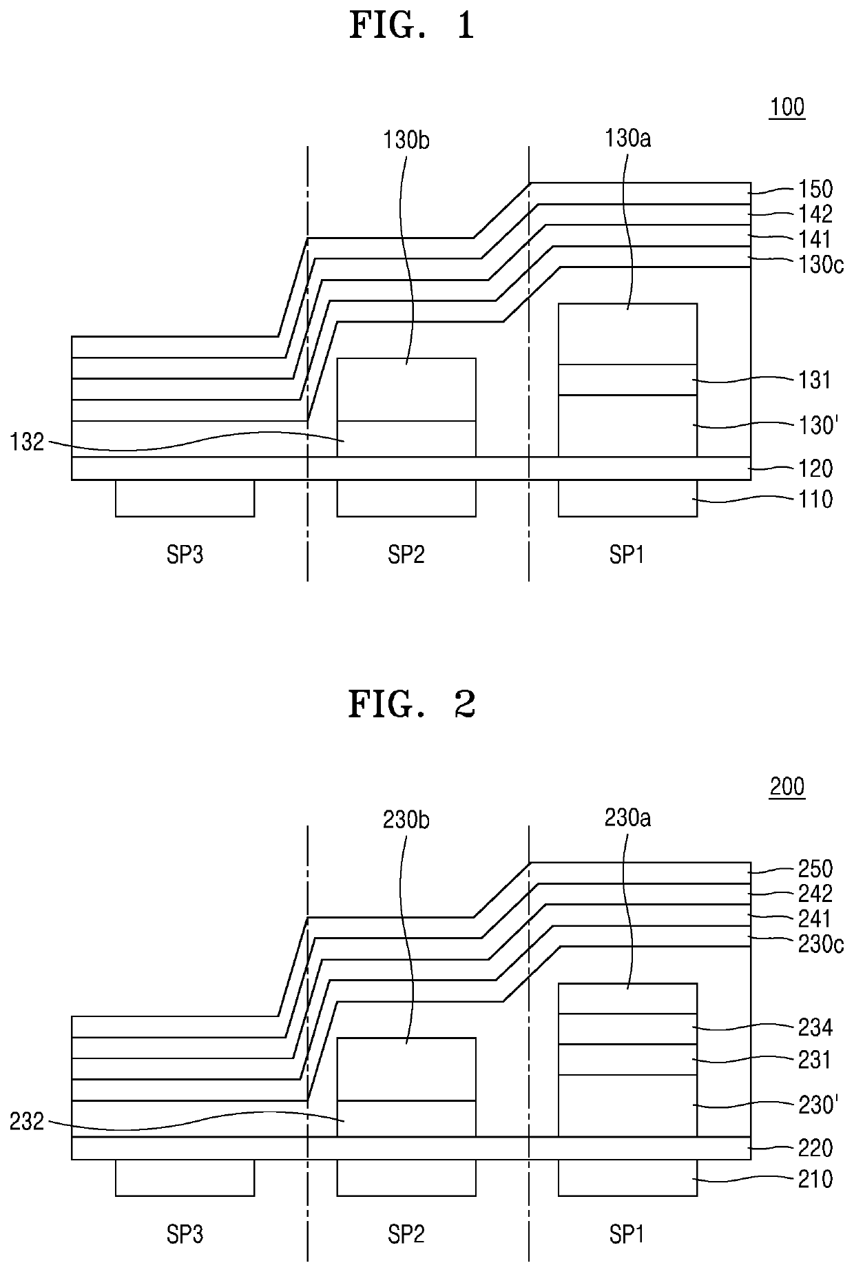
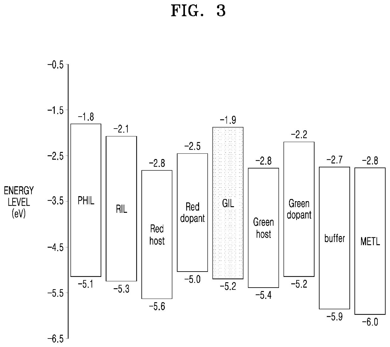
Light-emitting device
a technology of light-emitting devices and light-emitting holes, which is applied in the direction of solid-state devices, semiconductor devices, organic semiconductor devices, etc., can solve the problems of color mixing, a decrease in lifespan, and the effect of preventing or reducing color mixing
- Summary
- Abstract
- Description
- Claims
- Application Information
AI Technical Summary
Benefits of technology
Problems solved by technology
Method used
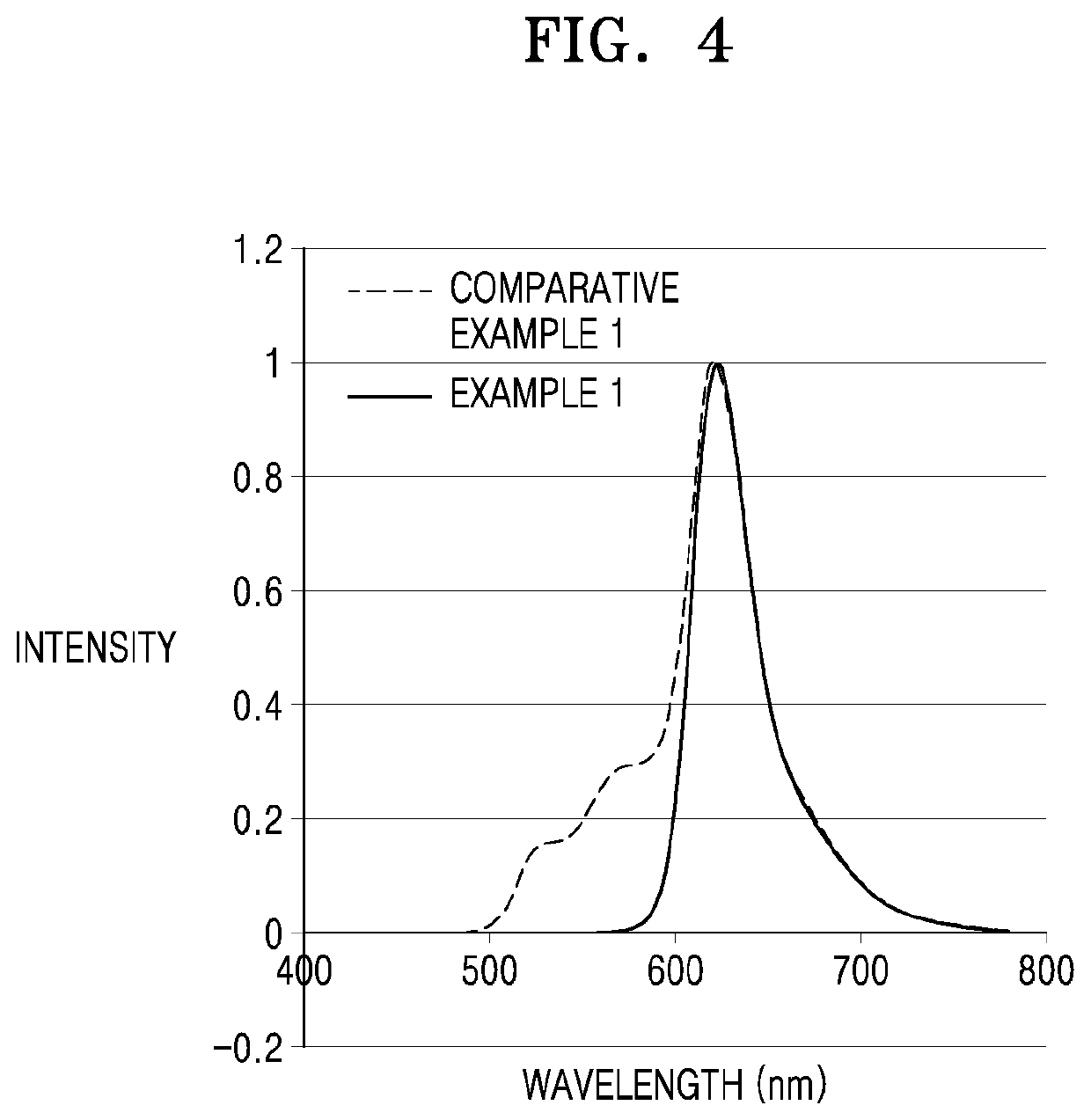
Image

Examples
example 1
[0290]As an anode, a 15 Ω / cm2 (1,200 Å) ITO glass substrate from Corning, Inc. of Corning, N.Y. (hereinafter “Corning”) was cut to a size of 50 mm×50 mm×0.7 mm, sonicated with isopropyl alcohol and pure water each for 5 minutes, and then cleaned by exposure to ultraviolet rays and ozone for 30 minutes. Then the resultant glass substrate was loaded onto a vacuum deposition apparatus.
[0291]Compound HT3 and HAT-CN were co-deposited at a weight ratio of 99:1 on the glass substrate to a thickness of 50 Å, and Compound HT3 was deposited thereon to a thickness of 220 Å, thereby forming a hole injection layer having a total thickness of 270 Å, and then m-MTDATA was vacuum-deposited on the hole injection layer to form a hole transport layer having a thickness of 50 Å.
[0292]Subsequently, in the blue subpixel area, Compound HT3 and HAT-CN were co-deposited at a weight ratio of 99:1 on the hole transport layer to a thickness of 100 Å, and Compound HT1 and F4-TCNQ were additionally deposited at ...
PUM
 Abstract
Description
Claims
Application Information