
Light-emitting device

a light-emitting device and light-emitting technology, applied in the field of light-emitting devices, can solve the problems of color mixing and a reduction in lifespan, the absence of the auxiliary layer of the single device, and the difficulty of securing a viewing angle, so as to prevent or reduce color mixing

Active Publication Date: 2020-09-17
SAMSUNG DISPLAY CO LTD
View PDF0 Cites 0 Cited by
  • Summary
  • Abstract
  • Description
  • Claims
  • Application Information

AI Technical Summary

Benefits of technology

The patent describes a new light-emitting device design that reduces driving voltage and increases luminance. It achieves this by using a common layer with two emission layers, but between them an intermediate layer is inserted to prevent color mixing. This design eliminates an auxiliary layer and reduces the high hole injection barrier, which could increase driving voltage and cause color mixing. In summary, the new design reduces the likelihood of color mixing and increases lifespan while maintaining high luminance.

Problems solved by technology

However, because the intermediate layer is in direct contact with the emission layer, an auxiliary layer in the single device is absent.
Furthermore, due to the absence of the auxiliary layer, a driving voltage may be increased by a high hole injection barrier, and electrons entering from the emission layer to the intermediate layer may not be blocked, thereby causing color mixing and a reduction in lifespan.
Thus, it is difficult to secure a viewing angle.

Method used


Image

  • Light-emitting device
  • Light-emitting device
  • Light-emitting device

Examples


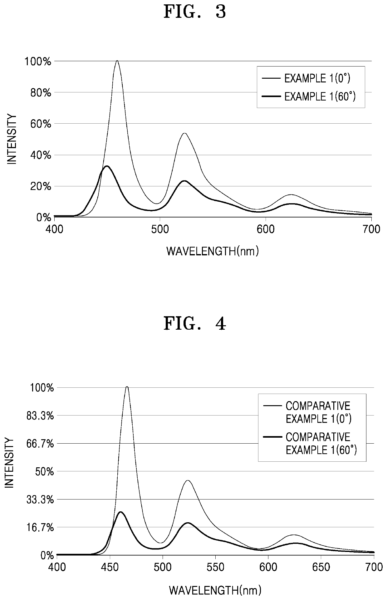
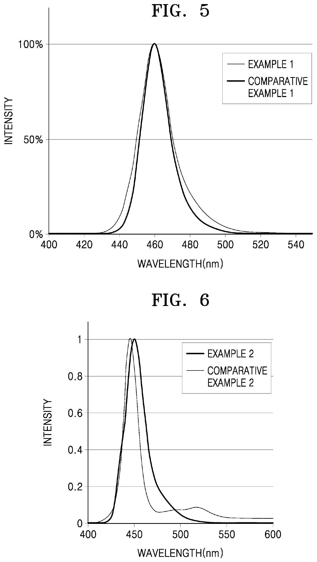
example 1

[0404]As an anode, a Corning 15 Ω / cm2 (1,200 Å) ITO glass substrate was cut to a size of 50 mm×50 mm×0.7 mm, sonicated with isopropyl alcohol and pure water each for 5 minutes, and then cleaned by exposure to ultraviolet rays and ozone for 30 minutes. Then, the ITO glass substrate was provided to a vacuum deposition apparatus.

[0405]HT3 and HAT-CN were co-deposited on the ITO glass substrate to a weight ratio of 99:1 to a thickness of 50 Å and HT3 was deposited thereon to a thickness of 220 Å to form a hole injection layer having a total thickness of 270 Å, and m-MTDATA was vacuum-deposited on the hole injection layer to form a hole transport layer having a thickness of 50 Å.

[0406]CBP (host) and Ir(ppy)3 (green dopant) were co-deposited on the hole transport layer to a weight ratio of 94:6 to form a green emission layer having a thickness of 250 Å as a common layer.

[0407]Then, HT3 and m-MTDATA were co-deposited on the green emission layer in a blue sub-pixel region to a weight ratio ...

example 2

[0420]As an anode, a Corning 15 Ω / cm2 (1,200 Å) ITO glass substrate was cut to a size of 50 mm×50 mm×0.7 mm, sonicated with isopropyl alcohol and pure water each for 5 minutes, and then cleaned by exposure to ultraviolet rays and ozone for 30 minutes. Then, the ITO glass substrate was provided to a vacuum deposition apparatus.

[0421]HT3 and HAT-CN were co-deposited on the ITO glass substrate to a weight ratio of 99:1 to a thickness of 50 Å and HT3 was deposited thereon to a thickness of 220 Å to form a hole injection layer having a total thickness of 270 Å, and m-MTDATA was vacuum-deposited on the hole injection layer to form a hole transport layer having a thickness of 50 Å.

[0422]CBP (host) and Ir(ppy)3 (green dopant) were co-deposited on the hole transport layer to a weight ratio of 94:6 to form a green emission layer having a thickness of 250 Å as a common layer.

[0423]Then, HT3 and m-MTDATA were co-deposited on the green emission layer in a blue sub-pixel region to a weight ratio ...

example 3

[0442]As an anode, a Corning 15 Ω / cm2 (1,200 Å) ITO glass substrate was cut to a size of 50 mm×50 mm×0.7 mm, sonicated with isopropyl alcohol and pure water each for 5 minutes, and then cleaned by exposure to ultraviolet rays and ozone for 30 minutes. Then, the ITO glass substrate was provided to a vacuum deposition apparatus.

[0443]HT3 and HAT-CN were co-deposited on the ITO glass substrate to a weight ratio of 99:1 to a thickness of 50 Å and HT3 was deposited thereon to a thickness of 220 Å to form a hole injection layer having a total thickness of 270 Å, and m-MTDATA was vacuum-deposited on the hole injection layer to form a hole transport layer having a thickness of 50 Å.

[0444]CBP (host) and Ir(ppy)3 (green dopant) were co-deposited on the hole transport layer to a weight ratio of 94:6 to form a green emission layer having a thickness of 250 Å as a common layer.

[0445]Then, HT3 and m-MTDATA were co-deposited on the green emission layer in a blue sub-pixel region to a weight ratio ...


PUM

PropertyMeasurementUnit
FWHMaaaaaaaaaa
FWHMaaaaaaaaaa
HOMO energy levelaaaaaaaaaa

Abstract

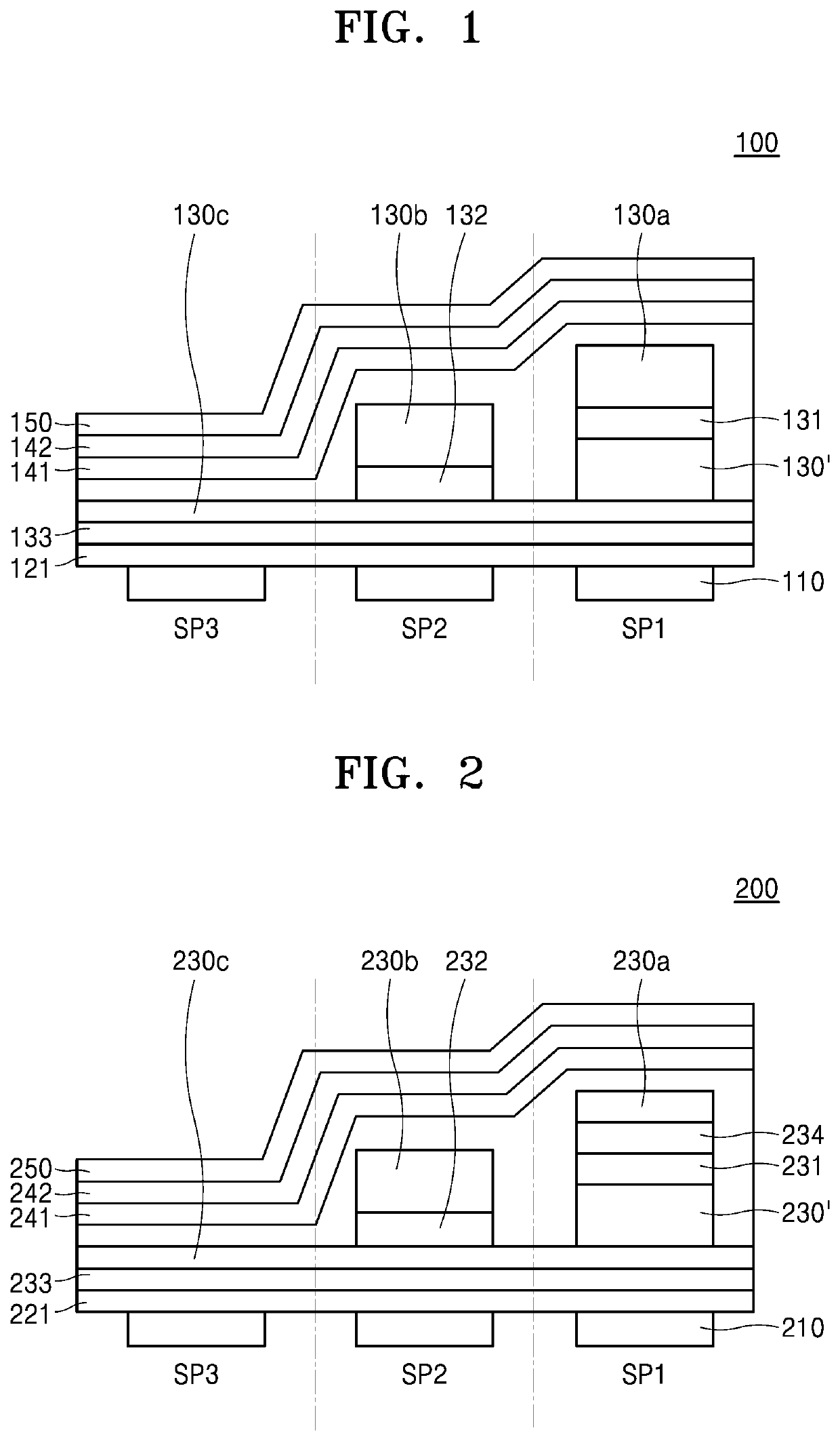
A light-emitting device includes: a plurality of first electrodes respectively in a first sub-pixel, a second sub-pixel, and a third sub-pixel; a second electrode facing the plurality of first electrodes; a first emission layer in the first sub-pixel and configured to emit a first color light; a second emission layer in the second sub-pixel and configured to emit a second color light; a first layer that is integrated with the first sub-pixel, the second sub-pixel, and the third sub-pixel; a first auxiliary layer between the first layer and the first emission layer; and a first intermediate layer between the first auxiliary layer and the first emission layer. The first emission layer includes a first host and a first dopant. The first dopant is configured to emit light having a full width at half maximum (FWHM) of about 35 nm or more.

Description

CROSS-REFERENCE TO RELATED APPLICATION[0001]This application claims priority to and the benefit of Korean Patent Application No. 10-2019-0028266, filed on Mar. 12, 2019, in the Korean Intellectual Property Office, the entire content of which is incorporated herein by reference.BACKGROUND1. Field[0002]One or more embodiments relate to a light-emitting device.2. Description of the Related Art[0003]Light-emitting devices may include an anode, a cathode, and an emission layer therebetween. Holes provided from the anode and electrons provided from the cathode recombine in the emission layer to produce excitons. These excitons transit (e.g., transition or relax) from an excited state to a ground state, thereby generating light.[0004]Light-emitting devices may be driven with a low voltage, may be implemented to be lightweight and thin, and may have excellent characteristics in terms of viewing angle, contrast, and response speed. Therefore, the application range of light-emitting devices h...

Claims


Application Information

Patent Timeline
Patent Type & Authority Applications(United States)
IPC IPC(8): H01L27/32H01L51/50C07F5/02C09K11/06H01L51/00
CPCH01L51/56H01L2251/5315H01L51/5004H01L51/008H01L51/5088H01L27/3211H01L2251/552C09K2211/1018H01L2251/558H01L51/504C07F5/027H01L27/3248H01L51/5092C09K11/06H01L51/5218H01L51/5234H01L51/506H01L51/5072H10K59/35H10K59/122H10K85/10H10K50/165H10K85/658H10K59/80518H10K50/17H10K59/875H10K85/321H10K50/131H10K2101/40H10K50/156H10K50/155H10K50/166H10K2101/30H10K85/649H10K85/6572H10K50/12H10K50/125H10K50/15H10K50/11H10K50/13H10K85/322H10K50/16H10K50/171H10K50/818H10K50/828H10K59/123H10K71/00H10K2102/351H10K2102/3026
Inventor JEON, PYUNGEUNOH, ILSOOLEE, BORAKANG, YUJINLEE, JUWON
Owner SAMSUNG DISPLAY CO LTD
Learn More