Transistor structure for electrostatic protection and method for manufacturing same

a transistor and electrostatic protection technology, applied in the field of semiconductor technology, can solve the problems of inability to play a role, premature damage of the device, and any time of electrostatic threat to the chip, and achieve the effect of improving the ability to protect against electrostatic damage and being easy to condu

Active Publication Date: 2021-07-08
JOULWATT TECH INC LTD
View PDF2 Cites 1 Cited by
  • Summary
  • Abstract
  • Description
  • Claims
  • Application Information

AI Technical Summary

Benefits of technology

[0025]According to the transistor structure for electrostatic protection and the method for manufacturing the same provided by the present disclosure, the first N-type well region, the P-type well region and the second N-type well region which are spaced in sequence are formed in the upper portion of the substrate, the first N+ region and the first P+ region are separately formed in the first N-type well region and the second N-type well region, the second P+ region close to the first N+ region and the second N+ region close to the first P+ region are formed in the P-type well region, so as to change a PN junction structure at each position of the transistor structure, such that when the transistor works, a conductivity feature of each position is changed, then the current path of the transistor structure under forward operation and reverse operation can be changed, the transistor structure may effectively suppress the base region stretching effect under forward operation and may provide better electrostatic protection capability under reverse operation, thereby improving the electrostatic protection capability of the entire transistor structure, and the process is easy to implement and operate.
[0026]Preferably, under forward operation, the current path between the second anode and the cathode is easier to be conductive to form a current channel for fully suppressing the base region stretching effect; and under reverse operation, a current channel is formed between the cathode and the first anode to provide better electrostatic protection capability.

Problems solved by technology

During manufacturing, packaging, testing and applying stages of a chip, certain charges will be accumulated in an external environment and an internal structure of the chip, resulting in electrostatic threat to the chip at any time.
Although an SCR structure has strong robustness in electrostatic protection under a human body model, the structure may cause premature damage of the device due to a base region stretching effect and cannot play a role in protection under an assembly charging model.

Method used


Image

  • Transistor structure for electrostatic protection and method for manufacturing same
  • Transistor structure for electrostatic protection and method for manufacturing same
  • Transistor structure for electrostatic protection and method for manufacturing same

Examples


second embodiment

[0066]FIG. 5 shows a sectional schematic diagram of a transistor structure for electrostatic protection according to the present disclosure.

[0067]FIG. 5 shows the transistor structure of the second embodiment, and compared with the transistor structure of the first embodiment, the transistor structure of this embodiment adds a third N+ region 533 in the P-type well region 503.

[0068]As shown in FIG. 5, the transistor structure comprises a substrate 501, a doped region 502 located in an upper portion of the substrate 501, and a P-type well region 503, a first N-type well region 505 and a second N-type well region 504 located in an upper portion of the doped region 502. The doped region 502 is an N-type shallowly doped region. The first N-type well region 505, the P-type well region 503 and the second N-type well region 504 are spaced in sequence, a first drift region 541 is provided between the first N-type well region 505 and the P-type well region 503, a second drift region 542 is p...

third embodiment

[0085]FIG. 7 shows a sectional schematic diagram of a transistor structure for electrostatic protection according to the present disclosure.

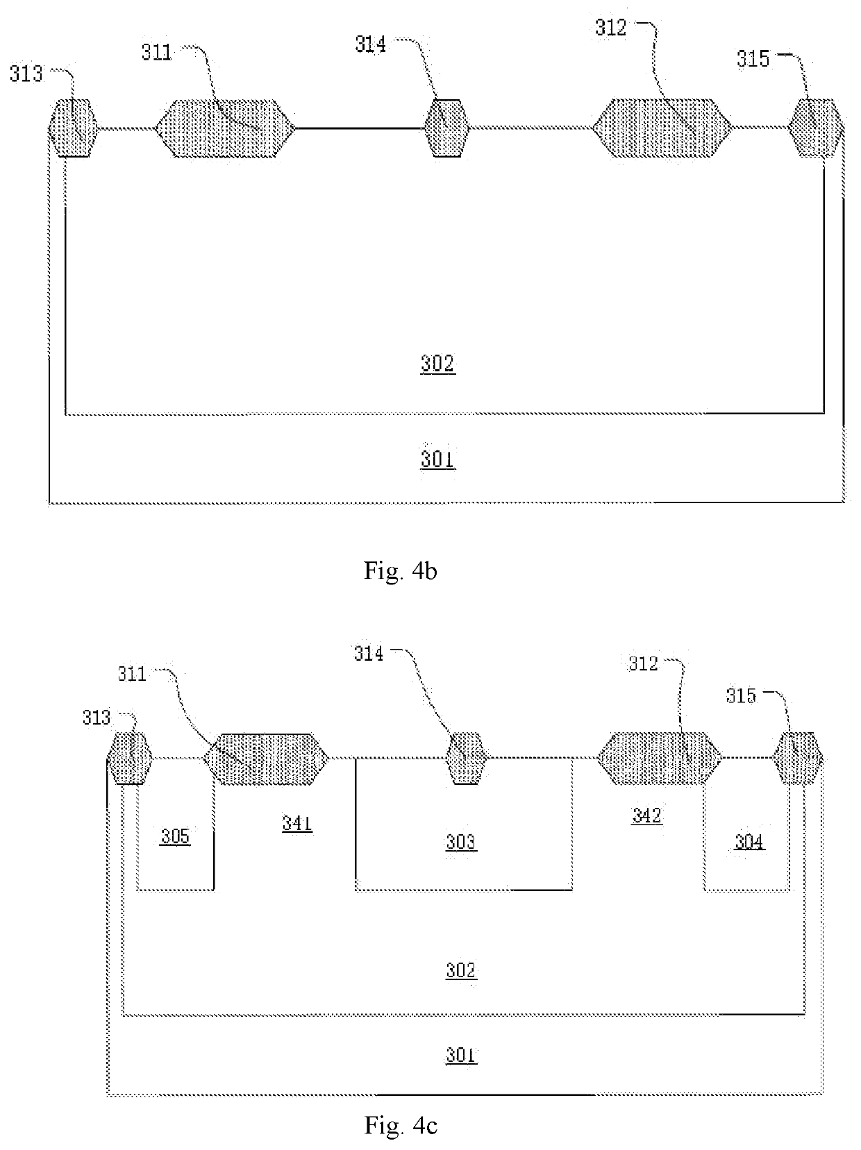
[0086]As shown in FIG. 7, the transistor structure comprises a substrate 701, a doped region 702 located in an upper portion of the substrate 701, and a P-type well region 703, a first N-type well region 705 and a second N-type well region 704 located in an upper portion of the doped region 702. The doped region 702 is an N-type shallowly doped region. The first N-type well region 705, the P-type well region 703 and the second N-type well region 704 are spaced in sequence, a first drift region 741 is provided between the first N-type well region 705 and the P-type well region 703, a second drift region 742 is provided between the second N-type well region 704 and the P-type well region 703, and the first drift region 741 has a length slightly larger than a length of the second drift region 742 have equal lengths.

[0087]Further, a first N+ region ...


PUM

PropertyMeasurementUnit
voltageaaaaaaaaaa
lengthaaaaaaaaaa
lengthsaaaaaaaaaa

Abstract

Disclosed are a transistor structure for electrostatic protection and a method for manufacturing same. The transistor structure comprises: a doped region in a substrate; field oxide layers; a first N-type well region, a P-type well region and a second N-type well region in the doped region and spaced in sequence; a first polycrystalline silicon layer and a second polycrystalline silicon layer covering part of the P-type well region; a first N+ region and a first P+ region respectively formed in the first N-type well region and the second N-type well region; a second N+ region and a second P+ region in the P-type well region. The second P+ region and the second N+ region are close to the first N+ region and the first P+ region, respectively. The structure may change a current path under forward/reverse operation; thus, a device keeps a good electrostatic protection capability and high robustness.

Description

FIELD OF TECHNOLOGY[0001]The present invention relates to a technical field of semiconductor technology, in particular to a transistor structure for electrostatic protection and a method for manufacturing the same.BACKGROUND[0002]Electro-Static Discharge (ESD), an objective natural phenomenon, accompanies an entire cycle of a product. During manufacturing, packaging, testing and applying stages of a chip, certain charges will be accumulated in an external environment and an internal structure of the chip, resulting in electrostatic threat to the chip at any time. Therefore, an ESD protective device needs to be placed on each pin in design of the chip for protecting a power-off state and a power-on state of the chip.[0003]In practical design, a silicon controlled rectifier (SCR) structure is often used as an ESD protective device for a high-voltage pin. Although an SCR structure has strong robustness in electrostatic protection under a human body model, the structure may cause premat...

Claims


Application Information

Patent Timeline
Patent Type & Authority Applications(United States)
IPC IPC(8): H01L27/02
CPCH01L27/0262
Inventor WANG, WEIHUAILU, YANG
Owner JOULWATT TECH INC LTD
Why Eureka
Try Eureka