Five junction multijunction metamorphic solar cell

a solar cell, multi-junction technology, applied in the direction of sustainable manufacturing/processing, climate sustainability, semiconductor devices, etc., can solve the problems of complex interdependence, complex and often unpredictable interactions, and tend to be more complex to manufacture, so as to increase the photoconversion efficiency

Active Publication Date: 2021-07-15
SOLAERO TECH CORP
View PDF5 Cites 3 Cited by
  • Summary
  • Abstract
  • Description
  • Claims
  • Application Information

AI Technical Summary

Benefits of technology

[0017]It is an object of the present disclosure to provide increased photoconversion efficiency in a multijunction solar cell for space applications over the operational life of the photovoltaic power system.
[0018]It is another object of the present disclosure to provide in a multijunction solar cell in which the selection of the composition of the subcells and their band gaps maximizes the efficiency of the solar cell at a predetermined temperature (in the range of 28 to 70 degrees Centigrade) and radiation environment in deployment in space at AM0 at a predetermined time after the initial deployment, such time being at least (i) one year; (ii) five years; (iii) ten years; or (iv) fifteen years, in a specific orbit or space mission.
[0039]In some embodiments, the selection of the composition of the subcells and their band gaps maximizes the efficiency of the solar cell at a predetermined temperature value (between 28 and 70 degrees Centigrade) at a predetermined time after the initial deployment in space, (the time of the initial deployment being referred to as the “beginning-of-life (BOL)”), such predetermined time being referred to as the “end-of-life (EOL)” time, and such time being at least one year.
[0040]In some embodiments, the selection of the composition of the subcells and their band gaps maximizes the efficiency of the solar cell at a predetermined low intensity (less than 0.1 suns) and low temperature value (less than 100 degrees Centigrade) in deployment in space at a predetermined time after the initial deployment in space, or the “beginning-of-life (BOL)”, such predetermined time being referred to as the “end-of-life (EOL)” time, and being at least one year.

Problems solved by technology

Compared to silicon, III-V compound semiconductor multijunction devices have greater energy conversion efficiencies and generally more radiation resistance, although they tend to be more complex to manufacture.
The overall power output and conversion efficiency of the solar cell are thereby affected in different and often unpredictable ways.
Such design variables are interdependent and interact in complex and often unpredictable ways.
Thus, such changes do not predictably lead to an increase in power output or solar cell efficiency.
Stated another way, focus on any single such material parameter in the design of a multijunction solar cell is not a viable design paradigm or calculus since each variable standing alone is NOT a simple “result effective variable” that can be mindlessly increased or decreased in order to achieve greater power output by those skilled in the art confronted with complex design specifications and practical operational considerations or related design objectives.

Method used


Image

  • Five junction multijunction metamorphic solar cell
  • Five junction multijunction metamorphic solar cell
  • Five junction multijunction metamorphic solar cell

Examples


second embodiment

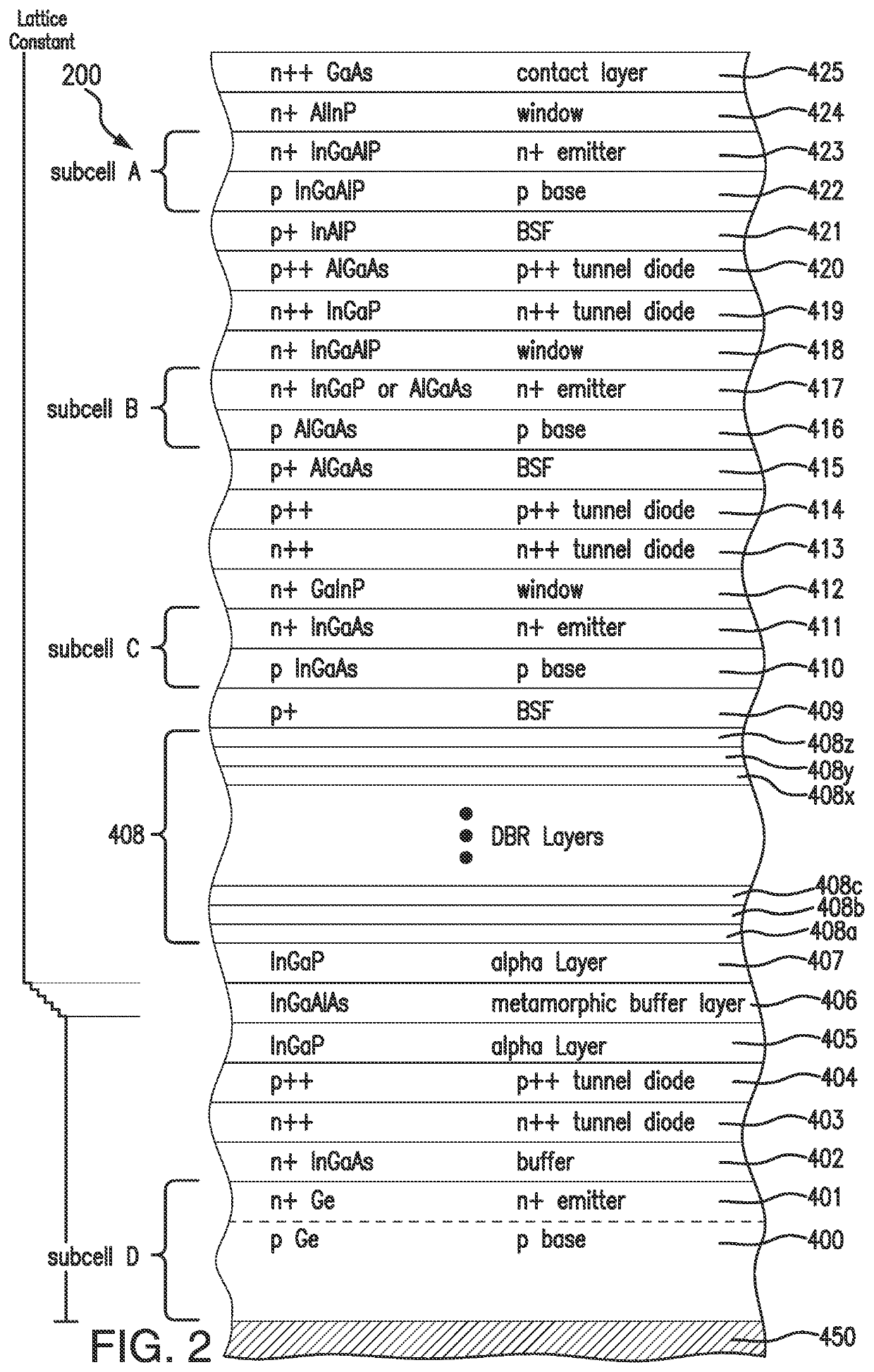
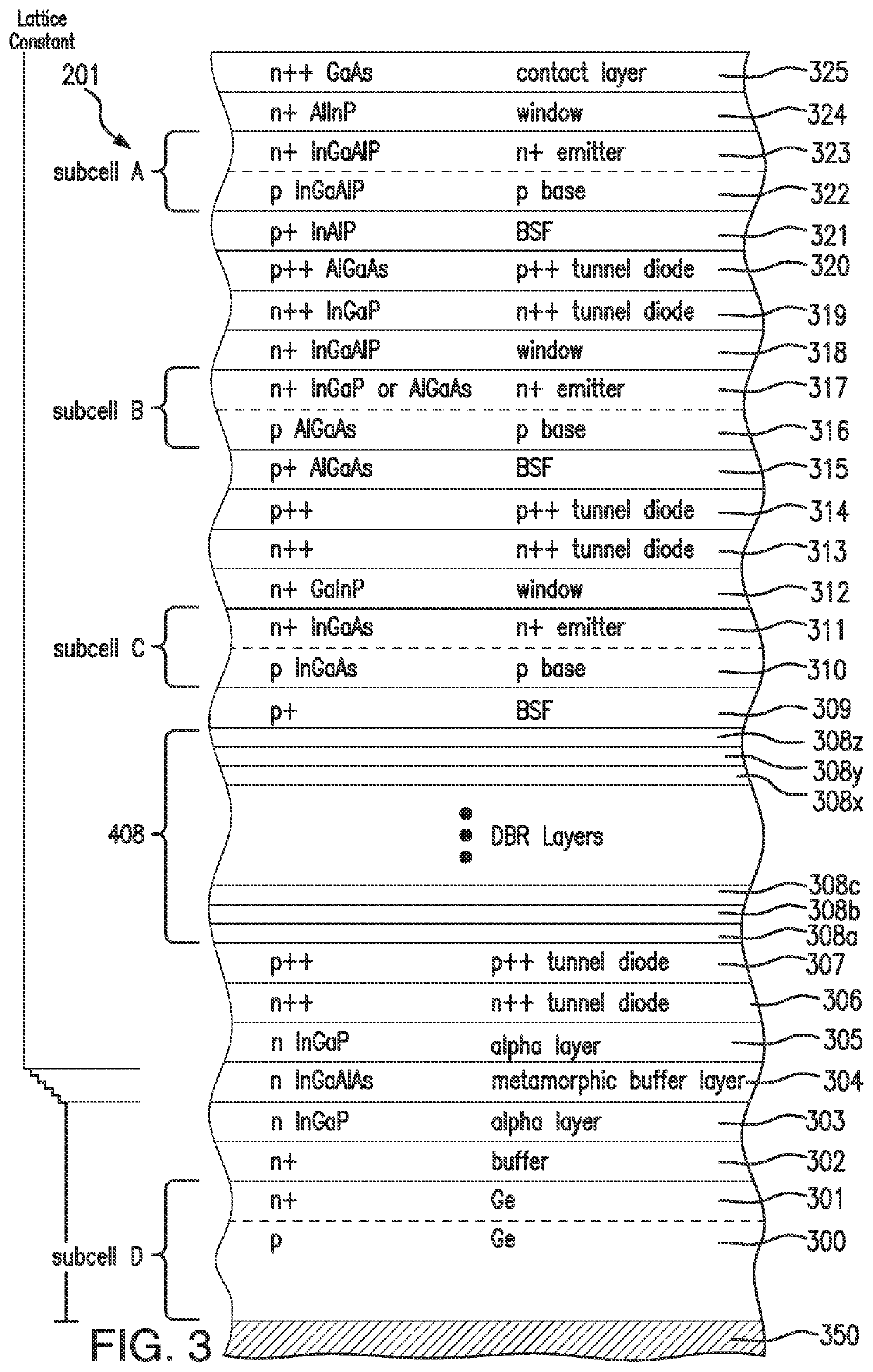
[0133]FIG. 3 is a cross-sectional view of a four junction solar cell 201 after several stages of fabrication including the growth of certain semiconductor layers on the growth substrate up to the contact layer, according to the present disclosure.

[0134]The second embodiment depicted in FIG. 3 is similar to that of the first embodiment depicted in FIG. 2 except that the metamorphic buffer layer 406 is disposed before the tunnel diode layers 403, 404 are deposited.

[0135]In FIG. 3, layers 650, 601, and 602 are substantially identical to that of layers 450, 401, and 402 in FIG. 2, and layers 608a, 608b, . . . 625 are substantially identical to that of layers 408a, 408b, . . . 425 in FIG. 2, so such description will not be repeated here for brevity.

[0136]Similarly, the first alpha layer 603, the metamorphic buffer layer 604, and second alpha layer 605 are similar to that of layers 405, 406 and 407 of FIG. 2, and the tunnel diode layer 606, 607 are similar to that of layer 403, 404 of FIG...

third embodiment

[0137]FIG. 4 is a cross-sectional view of a four junction solar cell 202 after several steps of fabrication including the growth of certain semiconductor layers on the growth substrate up to the contact layer, according to the present disclosure.

[0138]The third embodiment depicted in FIG. 4 is similar to that of the first embodiment depicted in FIG. 2 except that a quantum well structure 500 is included in subcell C.

[0139]In FIG. 4, in one embodiment quantum well layers 501a through 501n are disposed between the base layer 410 and the emitter layer 411 of subcell C.

[0140]Quantum well structures in multijunction solar cells are known from U.S. patent application Ser. No. 11 / 788,315, filed Apr. 18, 2007 hereby incorporated by reference.

[0141]In some embodiments, the plurality of quantum layers are “strained balanced” by incorporating alternating lower band gap (or larger lattice constant) compressively strained InGaAs and higher band gap (or smaller lattice constant) tensionally strai...


PUM

PropertyMeasurementUnit
band gapaaaaaaaaaa
band gapaaaaaaaaaa
band gapaaaaaaaaaa

Abstract

A five junction solar cell and its method of manufacture including an upper first solar subcell composed of a semiconductor material having a first band gap; a second solar subcell adjacent to said first solar subcell and composed of a semiconductor material having a second band gap smaller than the first band gap and being lattice matched with the upper first solar subcell; a third solar subcell adjacent to said second solar subcell and composed of a semiconductor material having a third band gap smaller than the second band gap and being lattice matched with the second solar subcell; a fourth solar subcell adjacent to said second solar subcell and composed of a semiconductor material having a fourth band gap smaller than the third band gap and being lattice matched with respect to the third solar subcell; a graded interlayer adjacent to the fourth solar subcell and having a fifth band gap greater than the fourth band gap; and a bottom solar subcell adjacent to the graded interlayer and being lattice mismatched from the fourth solar subcell and having a sixth band gap smaller than the fifth band gap.

Description

REFERENCE TO RELATED APPLICATIONS[0001]The present application is a divisional of U.S. patent application Ser. No. 16 / 722,732 filed Dec. 20, 2019 which is a divisional of U.S. patent application Ser. No. 15 / 681,144 filed Aug. 18, 2017, now U.S. Pat. No. 10,700,230.[0002]The present application is related to U.S. patent application Ser. No. 15 / 203,975 filed Jul. 7, 2016, and U.S. patent application Ser. No. 15 / 210,532 filed Jul. 14, 2016.[0003]This application is related to co-pending U.S. patent application Ser. No. 14 / 660,092 filed Mar. 17, 2015, which is a division of U.S. patent application Ser. No. 12 / 716,814 filed Mar. 3, 2010, now U.S. Pat. No. 9,018,521; which was a continuation in part of U.S. patent application Ser. No. 12 / 337,043 filed Dec. 17, 2008.[0004]This application is also related to co-pending U.S. patent application Ser. No. 13 / 872,663 filed Apr. 29, 2012 now U.S. Pat. No. 10,541,349, which was also a continuation-in-part of application Ser. No. 12 / 337,043, filed ...

Claims


Application Information

Patent Timeline
Patent Type & Authority Applications(United States)
IPC IPC(8): H01L31/0725H01L31/18H01L31/074
CPCH01L31/0725H01L31/1844H01L31/074H01L31/1808H01L31/1852Y02P70/50H01L31/06875H01L31/078Y02E10/544
Inventor DERKACS, DANIEL
Owner SOLAERO TECH CORP
Why Eureka
Try Eureka