Light emitting device

Pending Publication Date: 2021-07-15
SAMSUNG ELECTRONICS CO LTD
View PDF0 Cites 0 Cited by
  • Summary
  • Abstract
  • Description
  • Claims
  • Application Information

AI Technical Summary

Benefits of technology

[0006]Example embodiments provide a light emitting

Problems solved by technology

This may cause a low light ext

Method used


Image

  • Light emitting device
  • Light emitting device
  • Light emitting device

Examples


Example

[0042]Hereinafter, example embodiments will be explained in detail with reference to the accompanying drawings.

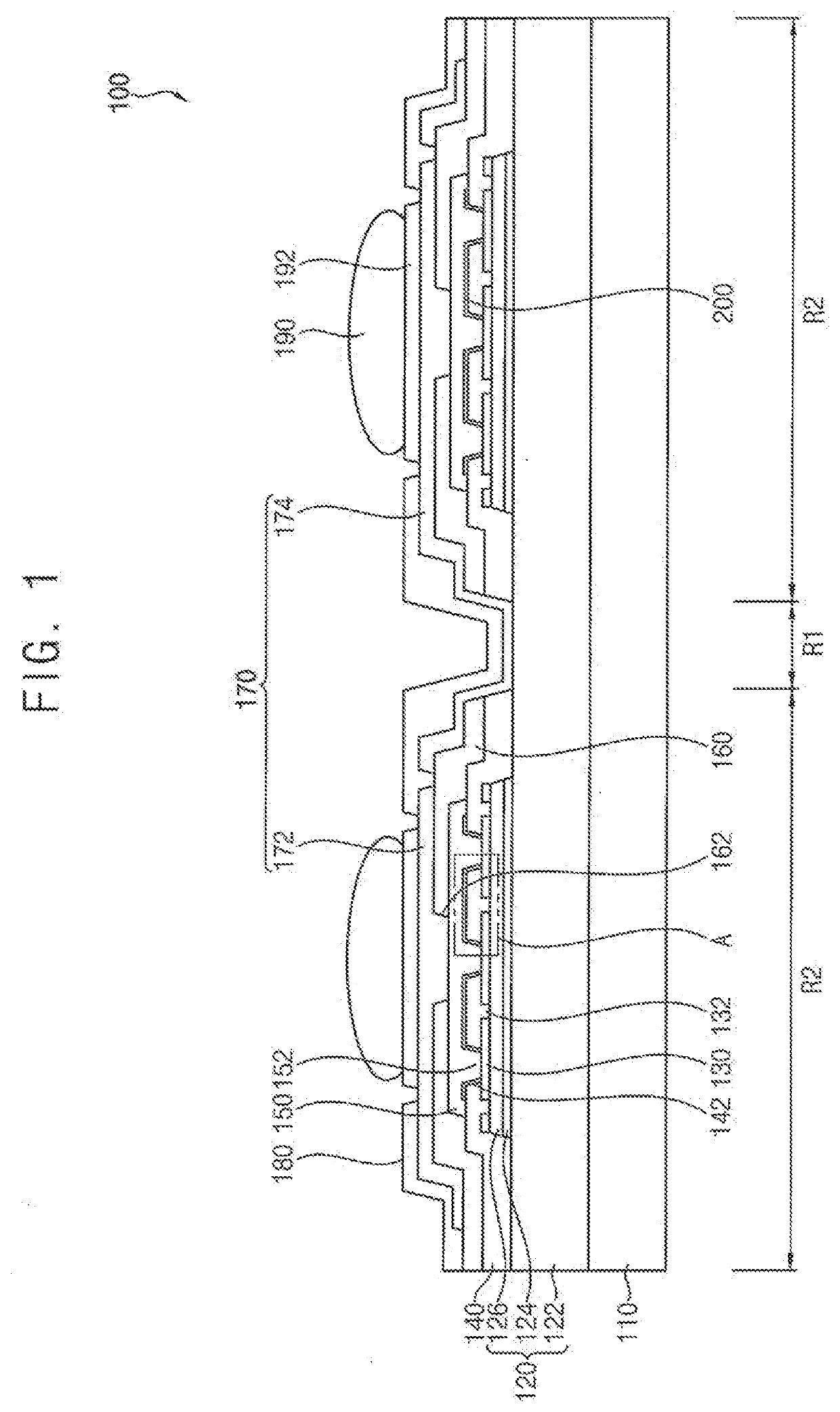
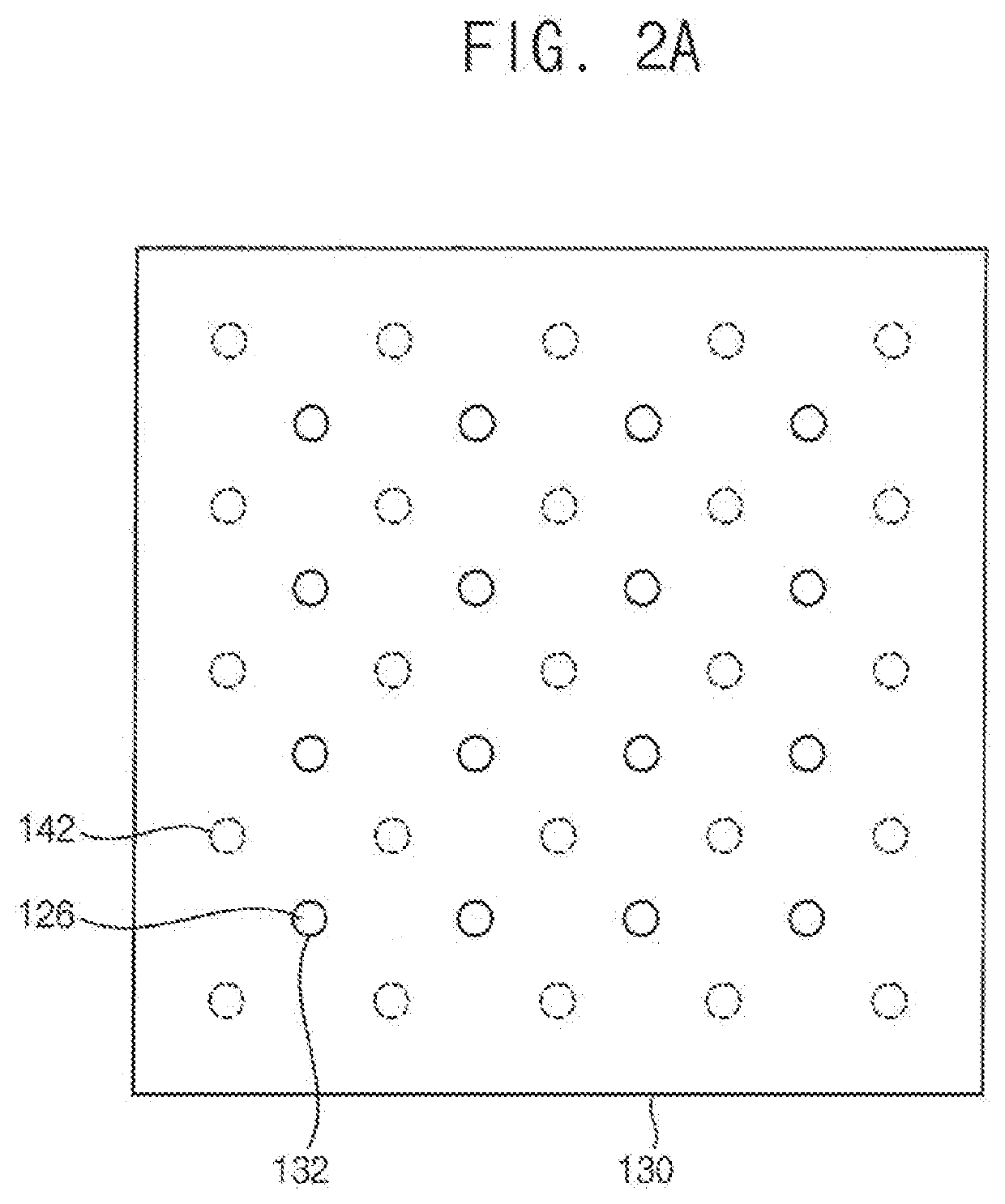
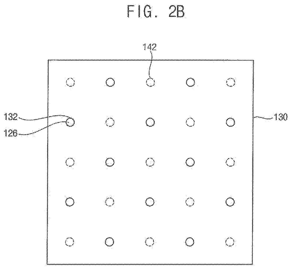
[0043]FIG. 1 is a cross-sectional view illustrating a light emitting device (LED) in accordance with example embodiments, FIGS. 2A to 2C are plan views illustrating example transparent electrodes of the LED in FIG. 1, and FIG. 3 is an enlarged cross-sectional view of a portion “A” in FIG. 1.

[0044]Referring to FIGS. 1 to 3, a light emitting device (LED) 100 of example embodiments may have a flip-chip structure. The flip-chip type LED 100 may include a growth substrate 110, a light emitting structure 120, a transparent electrode 130, a first insulation layer 140, a first electrode 150, a second insulation layer 160, a second electrode 170, a third insulation layer 180 and an adhesive layer 200.

[0045]The growth substrate 110 may include a sapphire (Al2O3) substrate, an SiC substrate, etc. However, the growth substrate 110 may include other materials besides the above-mentioned...


PUM


Abstract

A light emitting device may include a light emitting structure, a transparent electrode, a first insulation layer, a first electrode, a second insulation layer and a second electrode. The light emitting structure may include a first semiconductor layer, an activation layer and a second semiconductor layer sequentially stacked. The transparent electrode may be formed on an upper surface of the second semiconductor layer. The transparent electrode may have at least one opening. The first insulation layer may be formed on an upper surface of the transparent electrode to fill the at least one opening. The first electrode may be formed on an upper surface of the first insulation layer. The first electrode may include a contact extending through the first insulation layer and connected with the transparent electrode. The second insulation layer may be formed on an upper surface of the first electrode. The second electrode may be formed on an upper surface of the second insulation layer. The second electrode may be electrically connected with the first semiconductor layer.

Description

CROSS-REFERENCE TO RELATED APPLICATION[0001]This application is based on and claims priority under 35 USC § 119 to Korean Patent Application No. 10-2020-0005149, filed on Jan. 15, 2020, in the Korean Intellectual Property Office, the disclosure of which is incorporated by reference herein in its entirety.BACKGROUND1. Field[0002]The disclosure relates to a light emitting device. More particularly, example embodiments relate to a flip-chip type or a vertical type light emitting device.2. Description of Related Art[0003]Generally, a light emitting device (LED) may include a first semiconductor layer, an activation layer, a second semiconductor layer and a transparent electrode sequentially stacked. A first electrode may be electrically connected to the first semiconductor layer. A second electrode may be arranged over the transparent electrode.[0004]According to related arts, in order to optimize light extraction efficiency of a flip-chip type LED or a vertical LED, an insulation layer...

Claims


Application Information

Patent Timeline
IPC IPC(8): H01L33/38H01L33/44
CPCH01L33/38H01L33/42H01L2933/0016H01L33/44H01L33/62
Inventor KIM, TAEHUNSHIN, DONGMYUNGKIM, MINHOCHOI, MINWOOK
Owner SAMSUNG ELECTRONICS CO LTD
Why Eureka
Try Eureka