Electrode laminate and organic light emitting device element
- Summary
- Abstract
- Description
- Claims
- Application Information
AI Technical Summary
Benefits of technology
Problems solved by technology
Method used
Image
Examples
example 1
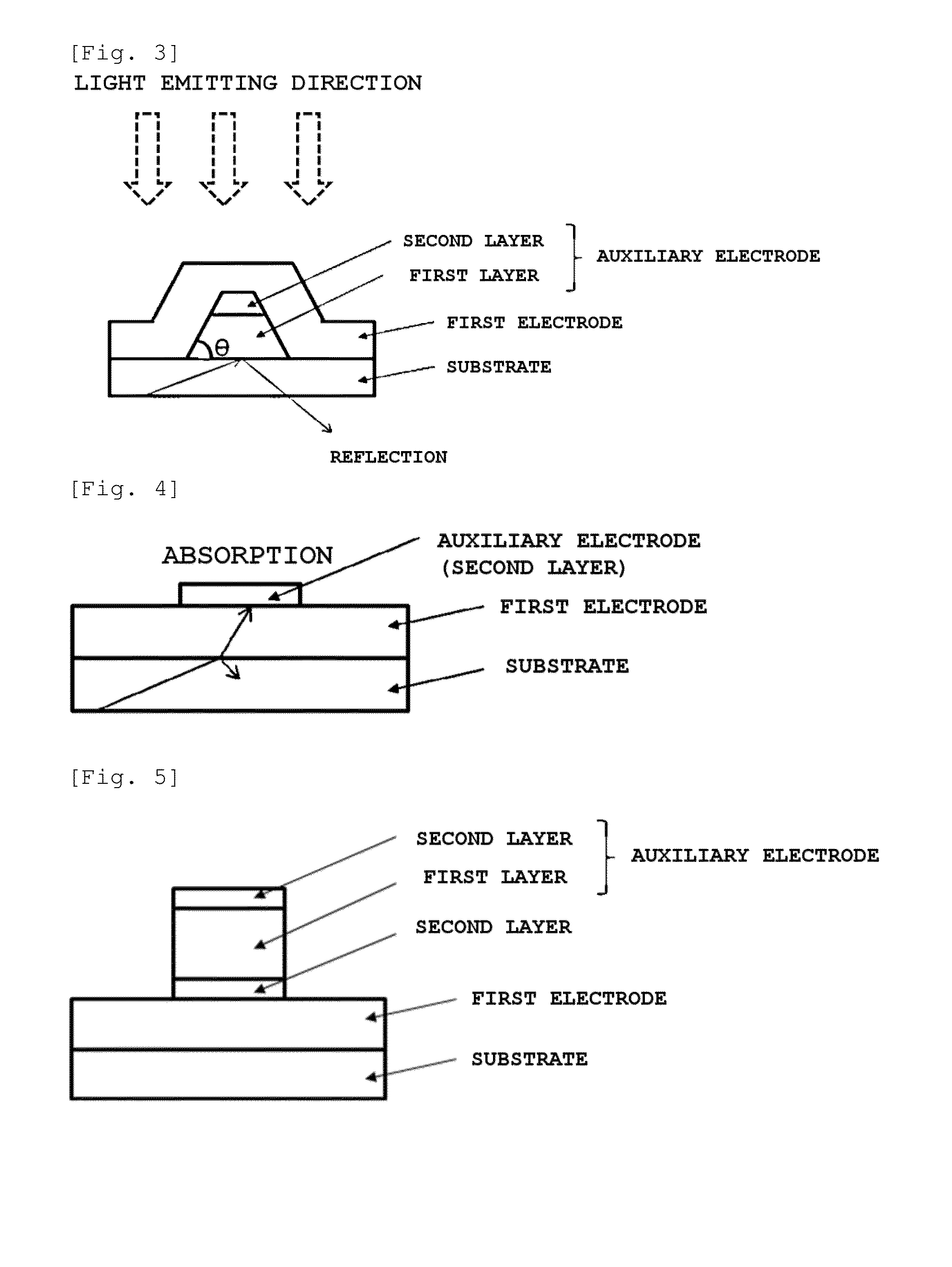
[0077]An auxiliary electrode pattern was formed on a glass substrate as a laminated structure of Al (thickness of 4,000 angstroms) and Mo (thickness of 500 angstroms), and an ITO layer was formed as a first electrode on the substrate and the auxiliary electrode pattern. Herein, a taper angle of the Al layer of the auxiliary electrode was within the range of 30° to 60°.
[0078]A SEM picture of the Al and Mo laminated structure prepared in the example is shown in FIG. 10. According to FIG. 10, the distance from one end unit of the lower surface of the Mo layer to one end unit of the upper surface of the Al layer is 0.1 micrometers. FIG. 11 is a mimetic diagram of SEM cross section of FIG. 10.
[0079]Subsequently, a light emitting layer and a second electrode were formed on the first electrode, and an organic light emitting device was manufactured.
example 2
[0080]Example 2 was carried out in the same manner as in Example 1 except that OCF (external light extraction layer) was additionally formed on the side opposite to the surface of the substrate on which the auxiliary electrode is provided.
PUM
 Abstract
Description
Claims
Application Information


