Check patentability & draft patents in minutes with Patsnap Eureka AI!

High-precision etching method

a high-precision, etching technology, applied in the field of semiconductors, can solve the problems of still encountered processing precision problems, and become more and more difficult to meet the requirements of smart electronic devices

Active Publication Date: 2021-07-22
INST OF MICROELECTRONICS CHINESE ACAD OF SCI
View PDF0 Cites 1 Cited by
  • Summary
  • Abstract
  • Description
  • Claims
  • Application Information

AI Technical Summary

Benefits of technology

The patent aims to prevent unwanted reactions between certain layers on a semiconductor material surface and a modifier. The modification layer formed by these reactions helps to stabilize the surface and prevent further damage.

Problems solved by technology

Although relatively small sizes of chips may have been achieved at present, problems with the processing precision are still encountered.
However, it is more and more difficult to satisfy the requirements for smart electronic devices, due to the substantial difference between the selectivity ratios of different materials.

Method used


Image

  • High-precision etching method
  • High-precision etching method
  • High-precision etching method

Examples


Embodiment Construction

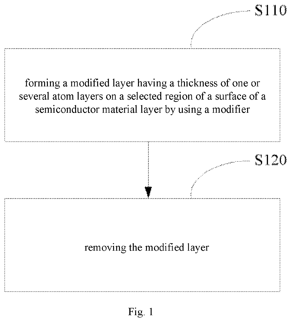
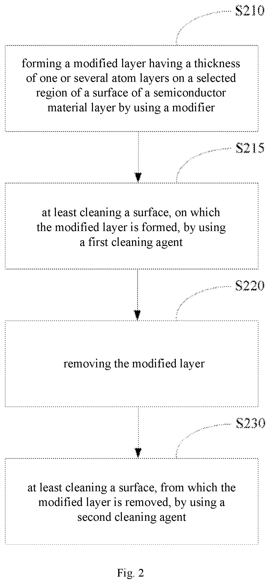
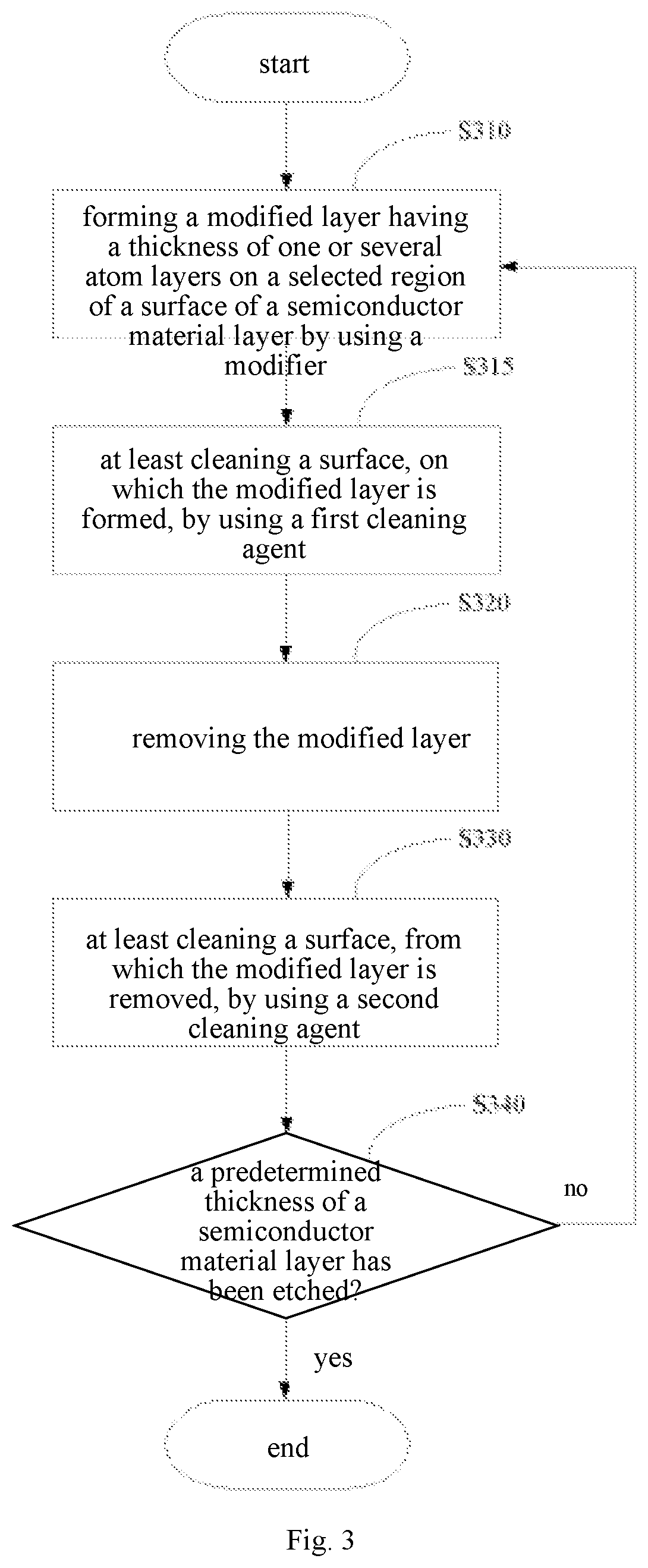
[0039]In order to enable objects, technical solutions, and advantages of the present application to be more obvious and clear, detailed descriptions are further made to the present application in conjunction with accompanying drawings below. It is to be noted that the following descriptions are only for the purpose of illustration, rather than limitation to this disclosure. In the description below, numerous specific details are set forth in order to provide a thorough understanding of this disclosure. However, it is apparent for those of ordinary skill in the art that it is not necessary to implement this disclosure by using these specific details. In other examples, well-known circuits, material, or methods are not specifically described in order to prevent this disclosure from being confused.

[0040]Throughout the description, references to “an embodiment”, “embodiments”, “an example”, or “examples”, or “some examples” mean that specific features, structures, or characteristics des...


PUM

PropertyMeasurementUnit
thicknessaaaaaaaaaa
thicknessaaaaaaaaaa
semiconductoraaaaaaaaaa

Abstract

An embodiment of the present disclosure provides an etching method, having the following steps: forming a modified layer having a thickness of one or several atom layers on a selected region of a surface of a semiconductor material layer by using a modifier; and removing the modified layer. When a semiconductor is processed, this method achieves precise control over the etching thickness and improves the etching rate at the same time.

Description

REFERENCE TO RELATED APPLICATION[0001]This application claims the priority of Chinese Patent Application 201810988644.4, entitled “High-Precision Etching Method,” filed on Aug. 28, 2018, the contents of which are incorporated herein by reference.TECHNICAL FIELD[0002]The present disclosure generally relates to the technical field of semiconductors, and more specifically, in particular to a high-precision etching method.BACKGROUND ART[0003]As the requirements for various smart electronic devices are increasing, the requirements for small-size and highly functional semiconductor chips increase therewith. Therefore, the extended large-scale requirements for transistors are accompanied.[0004]Although relatively small sizes of chips may have been achieved at present, problems with the processing precision are still encountered. For example, when a nanowire or a nanosheet is processed, the precise control over an etching process appears to be extremely important. Additionally, the selectiv...

Claims


Application Information

Patent Timeline
Patent Type & Authority Applications(United States)
IPC IPC(8): C23F1/16H01L21/306
CPCC23F1/16H01L21/30604H01L21/768H01L21/3065H01L21/306C09K13/08
Inventor ZHU, HUILONGYIN, XIAOGENLI, CHENDU, ANYANZHANG, YONGKUI
Owner INST OF MICROELECTRONICS CHINESE ACAD OF SCI
Features
  • R&D
  • Intellectual Property
  • Life Sciences
  • Materials
  • Tech Scout
  • Unparalleled Data Quality
  • Higher Quality Content
  • 60% Fewer Hallucinations
Learn More