Array substrate and display panel

a substrate and display panel technology, applied in the field of display technology, can solve the problems of inorganic materials easily broken by the display panel, oled to malfunction, etc., and achieve the effect of preventing device failure, facilitating process, and effectively preventing breaking

Inactive Publication Date: 2021-07-22
WUHAN CHINA STAR OPTOELECTRONICS SEMICON DISPLAY TECH CO LTD
View PDF0 Cites 3 Cited by
  • Summary
  • Abstract
  • Description
  • Claims
  • Application Information

AI Technical Summary

Benefits of technology

[0005]The object of this disclosure is to provide an array substrate. In this disclosure, all portions of a inorganic insulating layer (including a buffer layer, a first gate insulating layer, a second gate insulating layer, and a interlayer insulating layer) in the array substrate that do not function as insulation are removed from the inorganic insulating layer and only necessary portions for insulation are retained, thereby effectively preventing inorganic materials from being broken when a display panel having the array substrate is folded. Thus, a flexibility of the display panel is increased.
[0055]In the disclosure, forming a first contact hole and a second contact hole with a photomasks omits the number of photomasks in the process and simplifies the process. In addition, in the disclosure, a configuration of the inorganic insulating layers of the buffer layer, the first gate insulating layer, the second gate insulating layer, and the interlayer insulating layer for insulating is adjusted. Only portions of the inorganic insulating layers that functions as an insulating layer are retained, and remaining portions are entirely etched. All unnecessary portions (i.e., the unnecessary portions are portions that do not contact the active layer, the patterned first metal layer, etc., which do not function as an insulating layer) of the inorganic insulating layer (including the buffer layer, the first gate insulating layer, the second gate insulating layer, and the interlayer insulating layer) in the display area and the non-display area of the flexible substrate are removed, thereby minimizing the inorganic insulating layer in the curved portion (display area) of the display panel. Inorganic materials are effectively prevented from breaking when the display panel is folded. Moreover, in the disclosure, a groove is formed at a boundary between the display area and the non-display area of the flexible substrate on the organic dielectric layer, the planarization layer, and the pixel defining layer to expose the flexible substrate, thereby preventing device failure caused by organic matters entering into the display area with moisture.

Problems solved by technology

In conventional flexible OLEDs, an inorganic insulating layer (for example, a first gate insulating layer, a second gate insulating layer, and a interlayer insulating layer) generally covers a flexible substrate completely, and thus inorganic materials are easily broken when the display panel is folded.
It causes the OLEDs to malfunction.

Method used


Image

  • Array substrate and display panel
  • Array substrate and display panel
  • Array substrate and display panel

Examples


Embodiment Construction

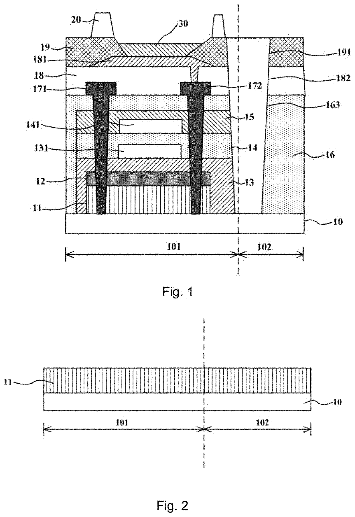
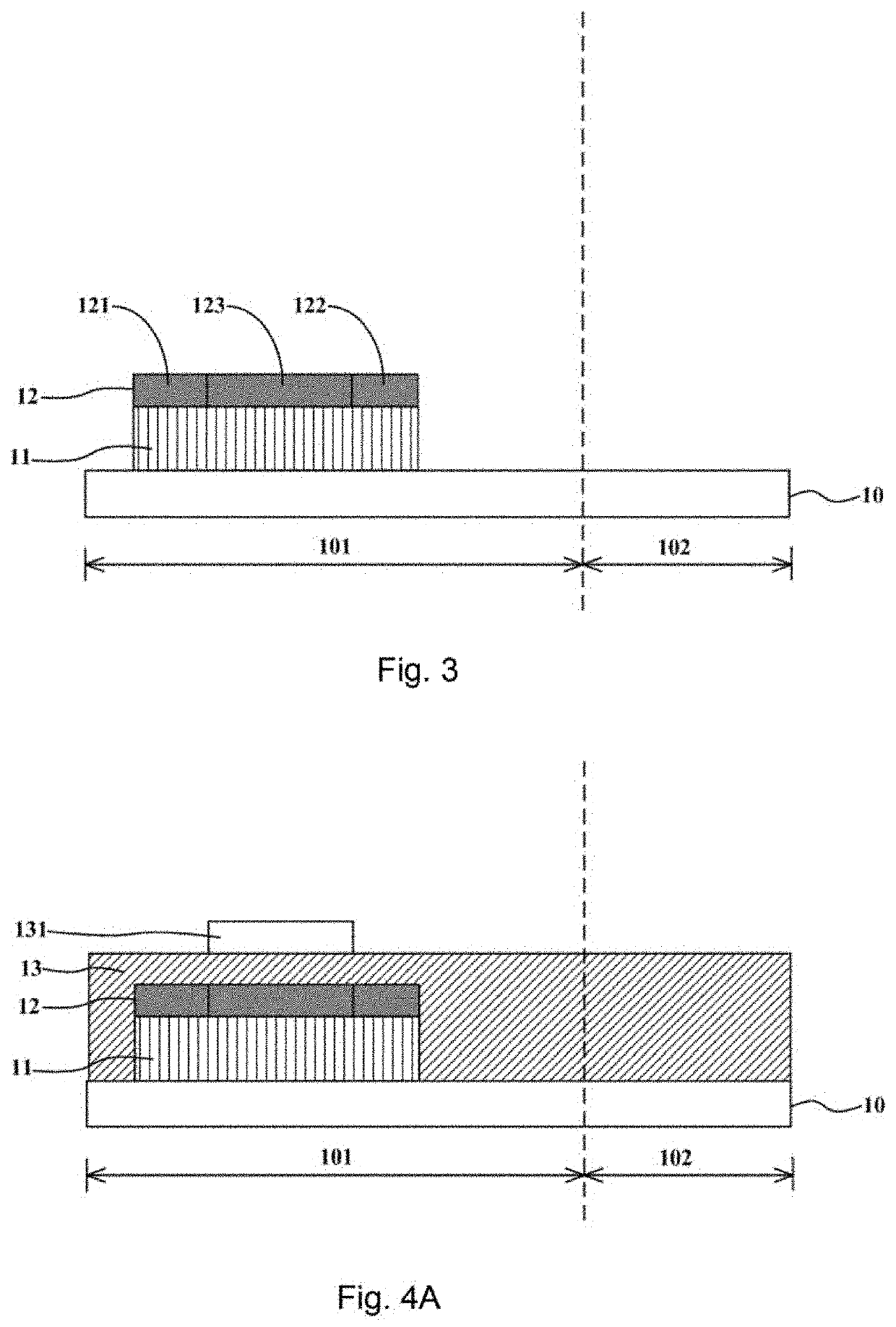
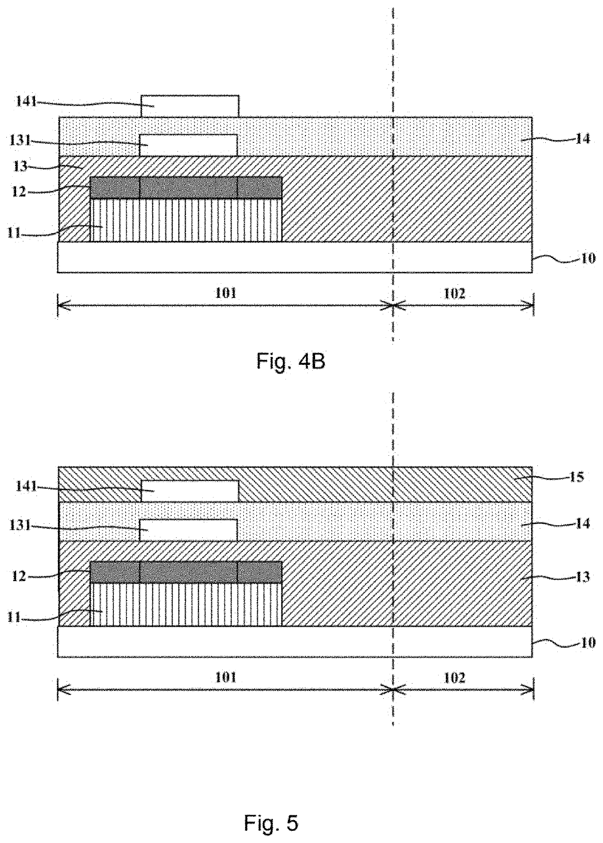
[0066]The specific details disclosed herein are merely representative and are intended to describe the purpose of the exemplary embodiments of this disclosure. This disclosure may be embodied in many and may not be construed as limited to the embodiments set forth herein.

[0067]This description of the exemplary embodiments is intended to be read in connection with the accompanying drawings, which are to be considered part of the entire written description. In the description, terms such as “lower”, “upper”, “horizontal”, “vertical”, “above”, “below”, “up”, “down”, “top”, and “bottom”, as well as derivatives thereof, should be construed to refer to the orientation as then described or as shown in the drawing under discussion. These terms are for convenience of description and do not require that the apparatus be constructed or operated in a particular orientation, and do not limit the scope of the disclosure. Referring to the drawings of the disclosure, similar components are labeled ...


PUM

PropertyMeasurementUnit
flexibleaaaaaaaaaa
areaaaaaaaaaaa
insulatingaaaaaaaaaa

Abstract

An array substrate, a display panel having the array substrate, a method of manufacturing the display panel, a display, and an electronic device having the same are provided. In the disclosure, a first contact hole and a second contact hole are formed by a photomask, thereby omitting the number of the photomasks in a process and simplifying the process. In addition, in the disclosure, all portions of the inorganic insulating layer (including a buffer layer, a first gate insulating layer, a second gate insulating layer, and a interlayer insulating layer) in the array substrate that do not function as insulation are removed from the inorganic insulating layer, thereby effectively preventing inorganic materials from being broken when the display panel is folded.

Description

FIELD OF INVENTION[0001]This disclosure relates to display technology, and more particularly to an array substrate, display panel, a method of manufacturing the array substrate, and a display and an electronic device having the same.BACKGROUND OF INVENTION[0002]In recent years, organic light-emitting diode (OLED) display panels have become very popular display devices, because OLED display devices have self-luminosity, wide viewing angles, fast response times, high luminous efficiency, wide color gamut, low energy consumption, are thinner, for application in large size and flexible panels, have a simple process, and have a low cost potential.[0003]In conventional flexible OLEDs, an inorganic insulating layer (for example, a first gate insulating layer, a second gate insulating layer, and a interlayer insulating layer) generally covers a flexible substrate completely, and thus inorganic materials are easily broken when the display panel is folded. It causes the OLEDs to malfunction.[...

Claims


Application Information

Patent Timeline
Patent Type & Authority Applications(United States)
IPC IPC(8): H01L51/00H01L27/32H01L51/56
CPCH01L51/0097H01L27/3258H01L27/1218H01L51/56H01L27/3262H10K59/12H10K59/124H10K77/111H10K59/1201H10K71/00H01L27/1248H01L27/124Y02E10/549Y02P70/50H10K59/1213H10K2102/311H01L27/1222H01L29/78645H01L29/78675
Inventor ZHAO, YU
Owner WUHAN CHINA STAR OPTOELECTRONICS SEMICON DISPLAY TECH CO LTD
Why Eureka
Try Eureka