Flip-chip bonding of light emitting devices and light emitting devices suitable for flip-chip bonding

a technology of light emitting devices and flip-chip bonding, which is applied in the field of flip-chip bonding of light emitting devices and light emitting devices suitable for flip-chip bonding, can solve the problems of unfavorable conventional techniques and predictably undesirable effects

Inactive Publication Date: 2005-05-03
CREELED INC +1
View PDF40 Cites 67 Cited by
  • Summary
  • Abstract
  • Description
  • Claims
  • Application Information

AI Technical Summary

Benefits of technology

[0011]In additional embodiments of the present invention, a light emitting device die having a mesa configuration on a substrate and an electrode on the mesa is attached to a submount in a flip-chip configuration by forming predefined pattern of conductive die attach material on at least one of the electrode and the submount and mounting the light emitting device die to the submount. The predefined pattern of conductive die attach material is selected so as to prevent the conductive die attach material from contacting sidewalls of the mesa or the substrate when the light emitting device die is mounted to the submount. The predefined pattern of conductive die attach material may provide a volume of die attach material that is less than a volume defined by an area of the electrode and a distance between the electrode and the submount.
[0014]In still further embodiments of the present invention, light emitting device die suitable for mounting on a submount includes a conducting substrate, such as a silicon carbide substrate, a gallium nitride based active region on the silicon carbide substrate and a first electrode on the gallium nitride based active region opposite the substrate. In some embodiments, the first electrode and the gallium nitride based active region form a mesa having sidewalls. A second electrode is provided on the silicon carbide substrate opposite the gallium nitride active region. A predefined pattern of conductive die attach material is provided on the first electrode opposite the gallium nitride active region that substantially prevents the conductive die attach material from contacting the sidewalls of the mesa and / or the substrate when the light emitting device die is mounted to the submount.
[0021]In further embodiments of the present invention, a light emitting device die includes a gallium nitride based active region having at least one region of a first conductivity type and a first electrode electrically coupled to the gallium nitride based active region. A region of semiconductor material of a second conductivity type is electrically coupled to the gallium nitride based active region. The second conductivity type is opposite to the first conductivity type. A predefined pattern of conductive die attach material is on the first electrode opposite the gallium nitride active region and configured to substantially prevent the conductive die attach material from contacting the region of semiconductor material of a second conductivity type when the light emitting device die is mounted to a submount.

Problems solved by technology

Namely, when a chip is flip-chip mounted on a conductive submount or package conventional techniques may not be possible.
This can cause the viscous conductive die attach material 26 to squeeze out and make contact with the n-type layers 14 and 10 in the device, thereby forming a Schottky diode connection that shunts the p-n junction in the active region with predictably undesirable results.

Method used


Image

  • Flip-chip bonding of light emitting devices and light emitting devices suitable for flip-chip bonding
  • Flip-chip bonding of light emitting devices and light emitting devices suitable for flip-chip bonding
  • Flip-chip bonding of light emitting devices and light emitting devices suitable for flip-chip bonding

Examples


Embodiment Construction

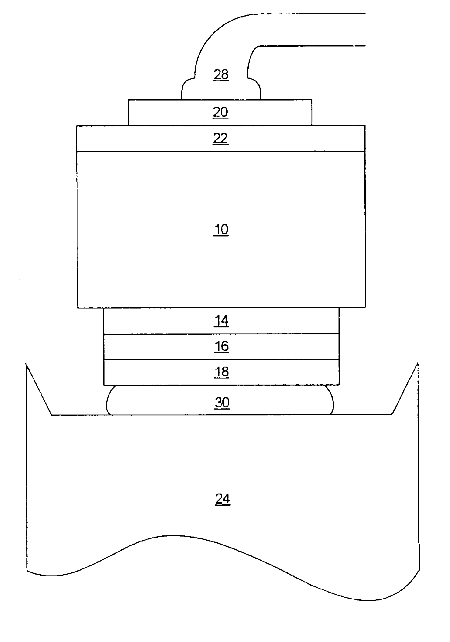
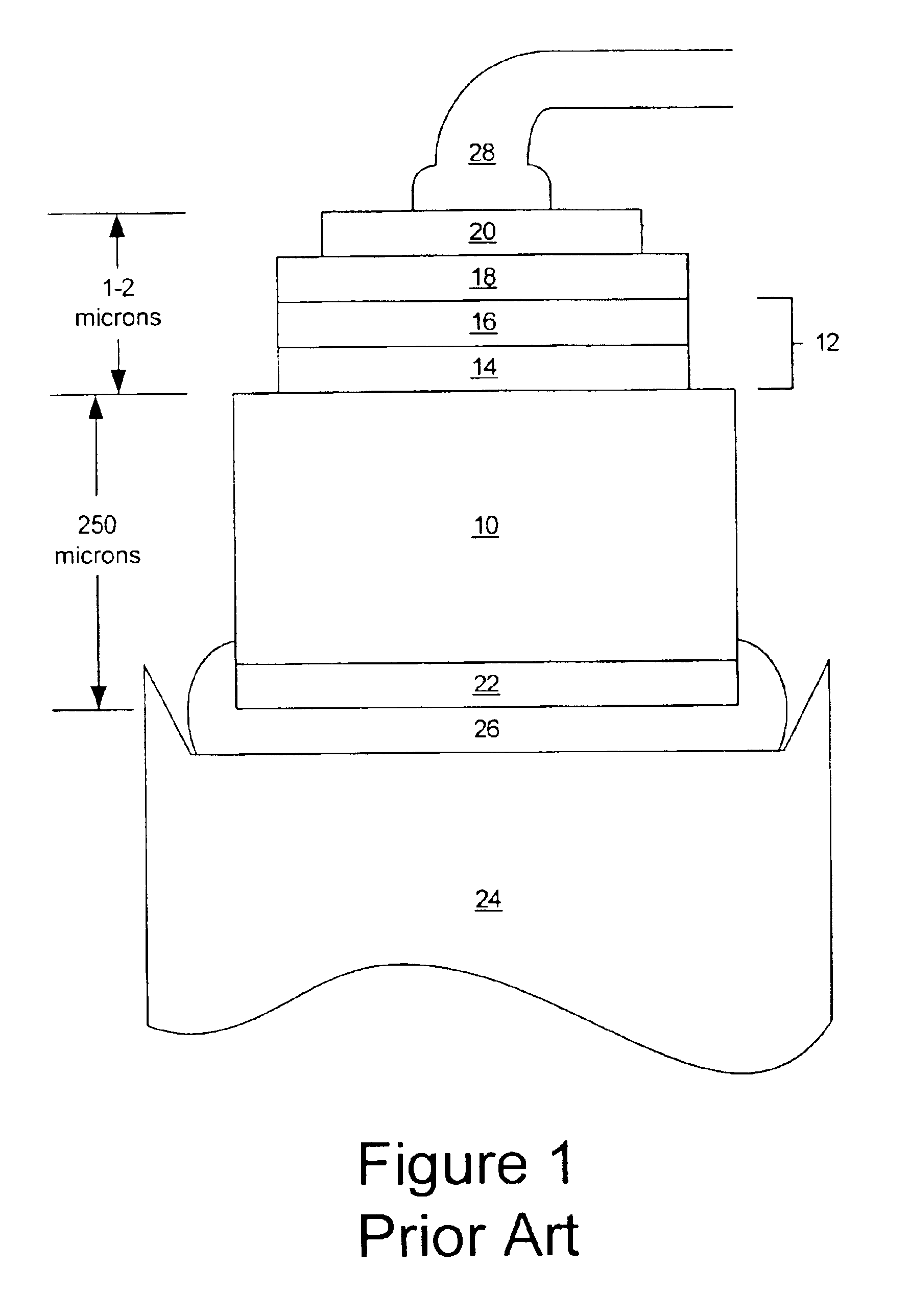
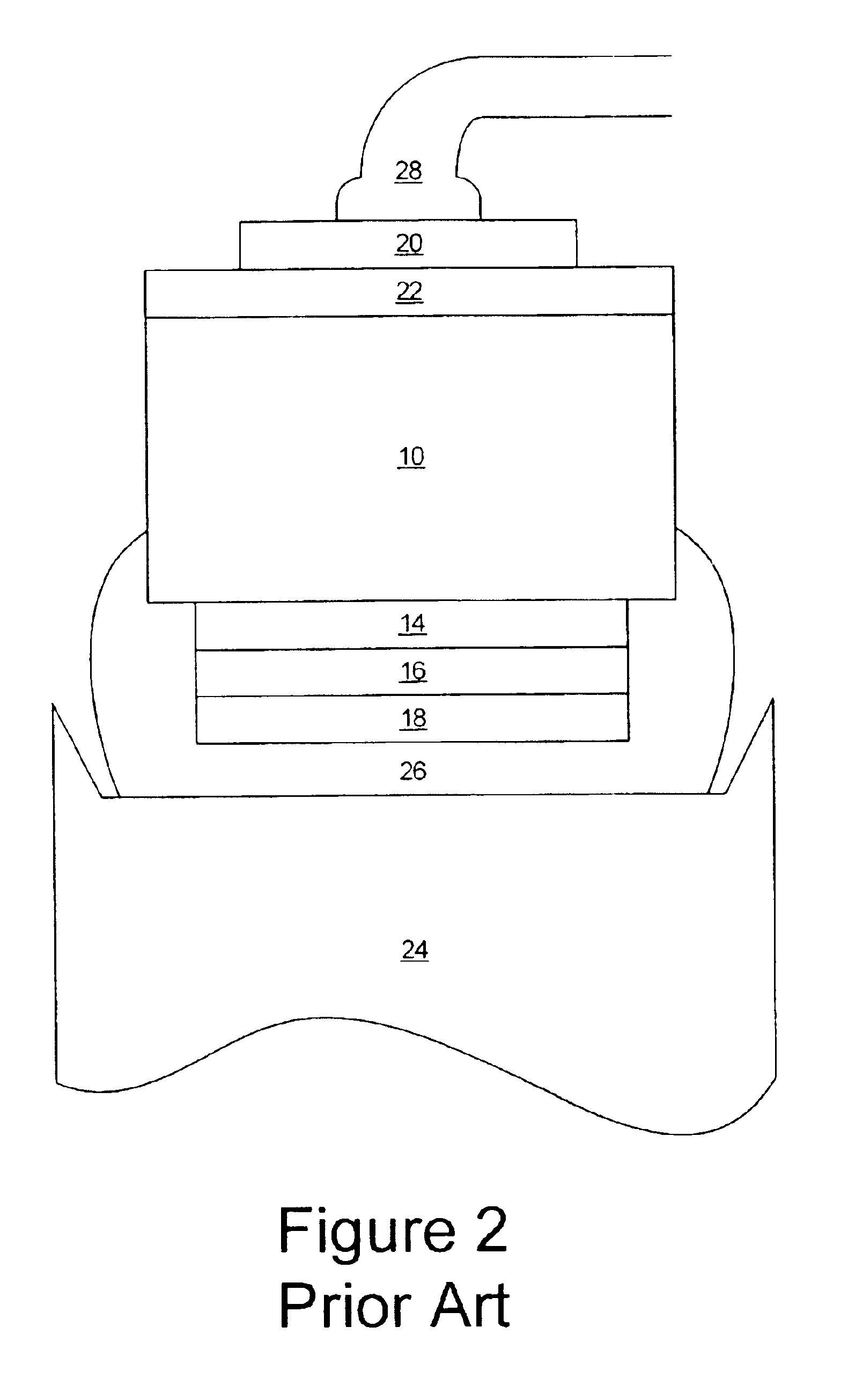
[0031]The present invention now will be described more fully hereinafter with reference to the accompanying drawings, in which preferred embodiments of the invention are shown. This invention may, however, be embodied in many different forms and should not be construed as limited to the embodiments set forth herein; rather, these embodiments are provided so that this disclosure will be thorough and complete, and will fully convey the scope of the invention to those skilled in the art. Like numbers refer to like elements throughout. Furthermore, the various layers and regions illustrated in the figures are illustrated schematically. As will also be appreciated by those of skill in the art, references herein to a layer formed “on” a substrate or other layer may refer to the layer formed directly on the substrate or other layer or on an intervening layer or layers formed on the substrate or other layer. Accordingly, the present invention is not limited to the relative size and spacing ...


PUM


Abstract

Light emitting device die having a mesa configuration on a substrate and an electrode on the mesa are attached to a submount in a flip-chip configuration by forming predefined pattern of conductive die attach material on at least one of the electrode and the submount and mounting the light emitting device die to the submount. The predefined pattern of conductive die attach material is selected so as to prevent the conductive die attach material from contacting regions of having opposite conductivity types when the light emitting device die is mounted to the submount. The predefined pattern of conductive die attach material may provide a volume of die attach material that is less than a volume defined by an area of the electrode and a distance between the electrode and the submount. Light emitting device dies having predefined patterns of conductive die attach material are also provided. Light emitting devices having a gallium nitride based light emitting region on a substrate, such as a silicon carbide substrate, may also be mounted in a flip-chip configuration by mounting an electrode of the gallium nitride based light emitting region to a submount utilizing a B-stage curable die epoxy. Light emitting device dies having a B-stage curable die epoxy are also provided.

Description

RELATED APPLICATIONS[0001]The present application claims priority from U.S. Provisional Patent Application Ser. No. 60 / 307,311 entitled “FLIP CHIP BONDING OF LIGHT EMITTING DIODES” and filed Jul. 23, 2001, the disclosure of which is incorporated herein by reference as if set forth fully.FIELD OF THE INVENTION[0002]The present invention relates to semiconductor devices, and more particularly to semiconductor devices mounted to a submount in a flip-chip configuration.BACKGROUND OF THE INVENTION[0003]GaN-based light emitting diodes (LEDs) typically comprise an insulating, semiconducting or conducting substrate such as sapphire or SiC on which a plurality of GaN-based epitaxial layers are deposited. The epitaxial layers comprise an active region having a p-n junction that emits light when energized. A typical LED is mounted substrate side down onto a submount, also called a package or lead frame (hereinafter referred to as a “submount”). FIG. 1 schematically illustrates a conventional L...

Claims


Application Information

Patent Timeline
Patent Type & Authority Patents(United States)
IPC IPC(8): H01L33/00H01L21/60H01L33/20H01L33/40H01L33/62
CPCH01L33/40H01L33/62H01L33/20H01L2224/04026H01L2224/48463H01L2224/73265H01L2924/12041H01L2924/01078H01L2924/01079H01L2924/12032H01L2224/291H01L2224/32245H01L2224/26175H01L2924/01057H01L2924/00014H01L2924/014H01L2924/00H01L33/38
Inventor SLATER, JR., DAVID B.BHARATHAN, JAYESHEDMOND, JOHNRAFFETTO, MARKMOHAMMED, ANWARANDREWSNEGLEY, GERALD H.
Owner CREELED INC
Why Eureka
Try Eureka