
Charge balance semiconductor device, in particular for high efficiency RF applications, and manufacturing process thereof

a semiconductor device and high-efficiency technology, applied in the direction of semiconductor devices/discharge tubes, electric devices, amplifiers, etc., can solve the problems of radio-frequency applications using superjunction mos devices, inability to meet, and inability to operate in the case of radio-frequency applications, etc., and achieve high efficiency

Pending Publication Date: 2021-09-02
STMICROELECTRONICS SRL
View PDF2 Cites 0 Cited by
  • Summary
  • Abstract
  • Description
  • Claims
  • Application Information

AI Technical Summary

Benefits of technology

This modification allows the superjunction power MOS device to operate at the desired resonance frequency, achieving higher breakdown voltage and comparable on-resistance to traditional superjunction devices, while maintaining low output capacitance at low voltages, suitable for high-efficiency RF applications.

Problems solved by technology

However, the use of superjunction MOS devices in radio-frequency applications clashes with the presence of parasitic components preventing operation thereof in real conditions.
In a superjunction power MOS device it is, however, problematical to satisfy the above conditions.
A study conducted by the applicant has shown that the plot of the output capacitance Cds of a superjunction device of the type shown in FIG. 2A leads to unacceptable operation in the case of radio-frequency applications.

Method used


Image

  • Charge balance semiconductor device, in particular for high efficiency RF applications, and manufacturing process thereof
  • Charge balance semiconductor device, in particular for high efficiency RF applications, and manufacturing process thereof
  • Charge balance semiconductor device, in particular for high efficiency RF applications, and manufacturing process thereof

Examples


Embodiment Construction

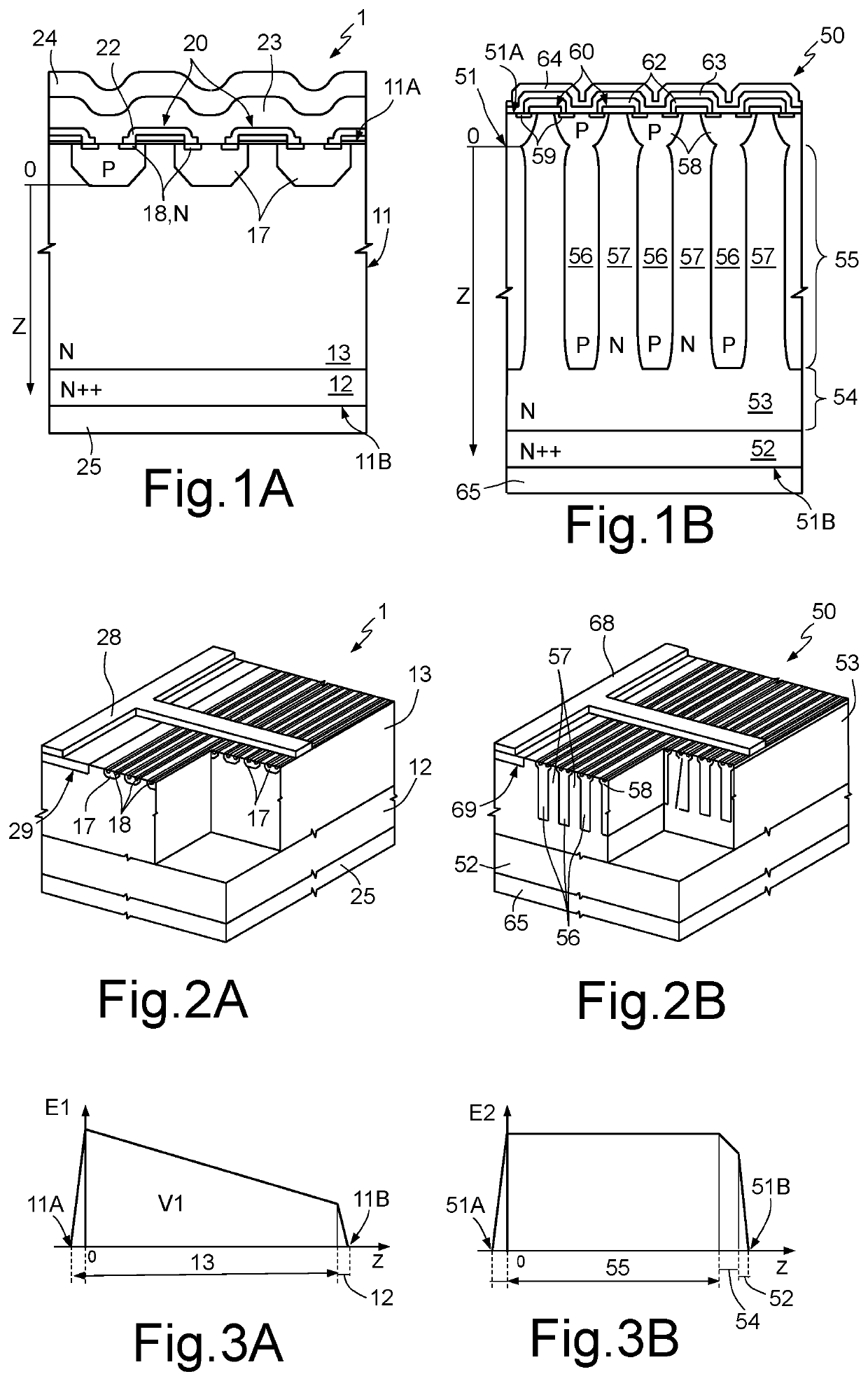
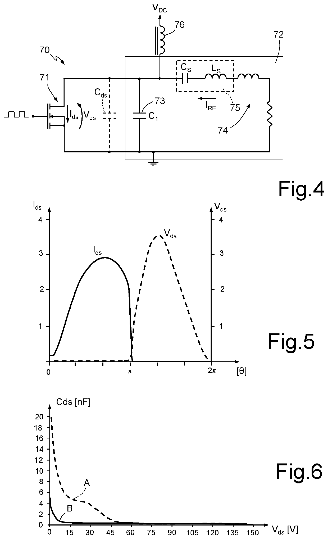
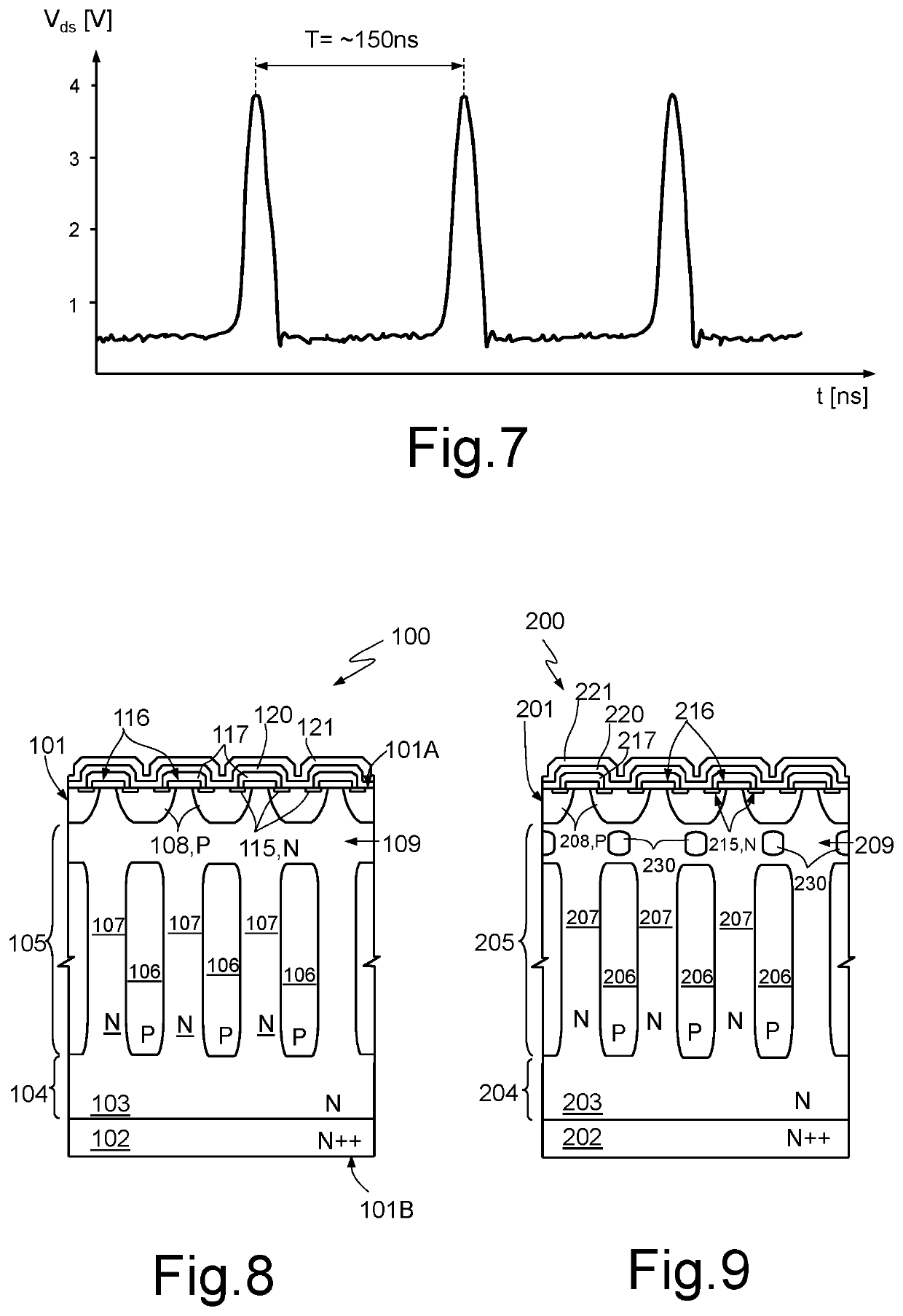
[0042]FIG. 8 shows an embodiment of a superjunction power MOS device, referred to hereinafter also as “device 100”.

[0043]The device 100 is integrated in a die comprising a body 101. The body 101 is of semiconductor material (such as Si, SiGe, SiC, Ge, GaN, GaAs, AlGaAs, InGaP or other suitable semiconductor material), has a top surface 101A and a rear surface 101B, presents a first conductivity type, for example N. The body 101 is typically formed by a substrate 102 having a higher doping concentration and an epitaxial layer 103, less doped, formed by successive growths. The epitaxial layer 103 forms a drain region 104 and a drift region 105. The drift region 105 accommodates a plurality of first columns 106 having a second conductivity type, here P, alternating with second columns 107 of N type, formed by the epitaxial layer 103. Body regions 108, here of P type, extend from the top surface 101A of the body 101 towards the top ends of the first columns 106, but are separated and te...


PUM

PropertyMeasurementUnit
voltagesaaaaaaaaaa
voltagesaaaaaaaaaa
frequencyaaaaaaaaaa

Abstract

A semiconductor MOS device having an epitaxial layer with a first conductivity type formed by a drain region and by a drift region. The drift region accommodates a plurality of first columns with a second conductivity type and a plurality of second columns with the first conductivity type, the first and second columns alternating with each other and extending on the drain region. Insulated gate regions are each arranged on top of a respective second column; body regions having the second conductivity type extend above and at a distance from a respective first column, thus improving the output capacitance Cds of the device, for use in high efficiency RF applications.

Description

BACKGROUNDTechnical Field[0001]The present disclosure relates in general to the field of power semiconductor devices, and more in particular to a power MOS device of the charge balance type (also referred to as superjunction device) for high efficiency RF applications, and to the manufacturing process thereof.Description of the Related Art[0002]As is known, power MOS semiconductor devices may generally be divided between horizontal structure devices and vertical structure devices. Amongst the latter, planar devices and devices having column structures (also referred to as charge balance or superjunction devices) may be distinguished.[0003]Vertical structure devices are shown in FIGS. 1A and 2A (for a power MOS device of a planar type) and in FIGS. 1B and 2B (for a superjunction power MOS device).[0004]With initial reference to FIGS. 1A and 2A (where the regions are not in scale, for sake of clarity), a planar MOS device 1 is integrated in a die comprising a body 11 of semiconductor ...

Claims


Application Information

Patent Timeline
Patent Type & Authority Applications(United States)
IPC IPC(8): H01L29/06H01L29/66H01L29/78H03F3/217
CPCH01L29/0634H01L29/66712H03F2200/451H03F3/2176H01L29/7811H01L29/7827H01L29/0847H01L29/66666H03F3/193H01L29/0623H01L29/7802
Inventor SCHILLACI, ANTONINOPONZIO, PAOLA MARIACAMMARATA, ROBERTO
Owner STMICROELECTRONICS SRL
Features
  • Generate Ideas
  • Intellectual Property
  • Life Sciences
  • Materials
  • Tech Scout
  • Unparalleled Data Quality
  • Higher Quality Content
  • 60% Fewer Hallucinations
Learn More