Mounting method and mounting device

a mounting method and mounting device technology, applied in semiconductor devices, semiconductor/solid-state device details, electrical apparatus, etc., can solve problems such as difficult prevent fluctuations in the temperature of heated semiconductor chips, circuit boards, mounting heads, etc., to achieve stable and accurate mounting, prevent thermal expansion and contraction, and prevent thermal expansion

Active Publication Date: 2021-09-09
TORAY ENG CO LTD
View PDF0 Cites 1 Cited by
  • Summary
  • Abstract
  • Description
  • Claims
  • Application Information

AI Technical Summary

Benefits of technology

[0038]With this configuration, fluctuation in the temperature of the heated semiconductor chip, circuit board, mounting head, and the like can be prevented, thermal expansion and contraction can be prevented in all of the members related to mounting, and stable, accurate mounting can be carried out.
[0039]The mounting method and mounting device of the present invention allow semiconductor chip to be stably and accurately mounted on a circuit board.

Problems solved by technology

However, with the invention described in Patent Literature 1, there is a possibility that the adhesive layer will be left behind on the semiconductor chip, which is a problem in that variance in the amount of this adhesive layer makes stable mounting difficult.

Method used


Image

  • Mounting method and mounting device
  • Mounting method and mounting device
  • Mounting method and mounting device

Examples


first embodiment

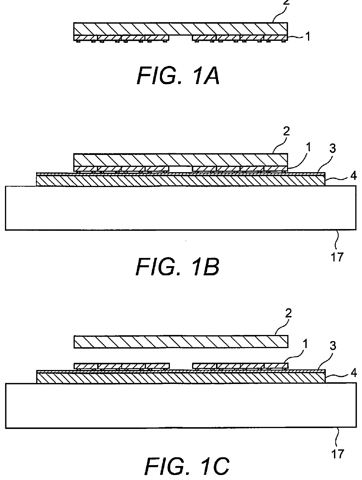
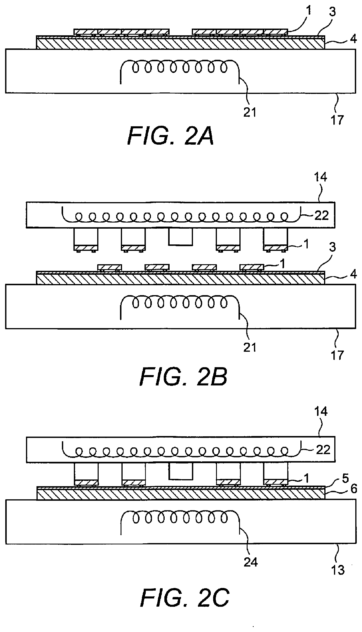
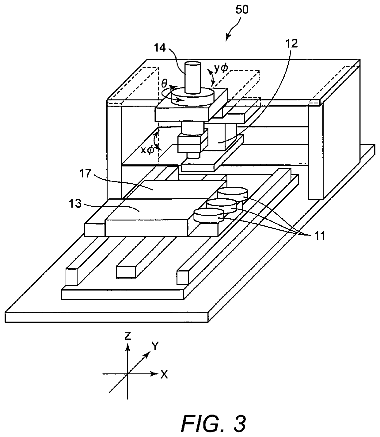
[0053]A first embodiment of the present invention will be described through reference to FIGS. 1A to 5B. FIGS. 1A, 1B and 1C are diagrams illustrating the first half of a mounting method in the first embodiment of the present invention. FIGS. 2A, 2B and 2C are diagrams illustrating the second half of the mounting method in the first embodiment of the present invention. FIG. 3 is a diagram illustrating a mounting device in the first embodiment of the present invention. FIG. 4 is a diagram illustrating a head portion of the mounting device in the first embodiment of the present invention. FIGS. 5A and 5B are diagrams illustrating the adjustment of the parallelism of the head of the mounting device in the first embodiment of the present invention.

[0054]In the present invention, of the two main faces of a semiconductor chip, the face held by the carrier substrate shall be termed the first face, the face on the opposite side from the first face is defined as the second face, and it shall...

second embodiment

[0082]A second embodiment of the present invention differs from the first embodiment in that a head 114 that picks up the semiconductor chips 1 from the adhesive sheet 4 whose adhesive strength has been reduced picks up the semiconductor chips 1 one at a time. Just as with the head 14 in the first embodiment, the head 114 comprises a heating component comprising a heater 122.

[0083]The mounting method in the second embodiment of the present invention will be described through reference to FIGS. 6A to 6C. FIGS. 6A, 6B and 6C are diagrams illustrating the second half of a mounting method in the second embodiment of the present invention. The first half of the mounting method in the second embodiment is the same as in the first embodiment. In the second half of the mounting method in the second embodiment, the adhesive strength reduction step shown in FIG. 6A is executed as in the first embodiment. In the adhesive strength reduction step, the adhesive strength of the adhesive film 3 of ...

third embodiment

[0087]A third embodiment of the present invention differs from the first and second embodiments in that the semiconductor chips I are pressed in order to prevent the semiconductor chips 1 from scattering due to the reduction in the adhesive strength of the adhesive sheet 4 in the adhesive strength reduction step.

[0088]The third embodiment of the present invention will be described through reference to FIG. 7. FIG. 7 is a diagram illustrating the adhesive strength reduction step in the third embodiment of the present invention. In the third embodiment, as shown in FIG. 7, a mounting device 50 is provided with a pressing component 231, and can be pressed and moved in the Z direction by a drive mechanism (not shown). In the adhesive strength reduction step, the pressing component 231, which has been heated to the specific temperature in the adhesive strength reduction step described in the first embodiment, presses on the semiconductor chips 1 held by the adhesive sheet 4, the semicond...


PUM

PropertyMeasurementUnit
sizeaaaaaaaaaa
temperatureaaaaaaaaaa

Abstract

A mounting method is a method for mounting a diced semiconductor chip having a first face that is held on a carrier substrate and a second face that is an opposite face of the first face on a circuit board placed on a mounting table. The mounting method includes affixing the second face of the semiconductor chip to an adhesive sheet, removing the carrier substrate from the semiconductor chip, reducing an adhesive strength of the adhesive sheet, and mounting the semiconductor chip on the circuit board by holding a first face side of the semiconductor chip with a head to separate the semiconductor chip from the adhesive sheet, and joining a second face side of the semiconductor chip to the circuit board.

Description

CROSS-REFERENCE TO RELATED APPLICATIONS[0001]This application is a U.S. National stage of International Application No. PCT / JP2017 / 030101 filed on Aug. 23, 2017. This application claims priority to Japanese Patent Application Nos. 2016-163968 filed on Aug. 24, 2016 and 2017-009030 filed on Jan. 21, 2017 with Japan Patent Office. The entire disclosures of Japanese Patent Application Nos. 2016-163968 and 2017-009030 are hereby incorporated herein by reference.BACKGROUNDField of the Invention[0002]The present invention relates to a mounting method and a mounting device for stably and accurately mounting a semiconductor chip. Background Information[0003]In order to reduce cost, semiconductor chips have been made smaller, and efforts have been made to mount these miniaturized semiconductor chips accurately. In particular, in LEDs used in displays, semiconductor chips measuring 50 μm×50 μm or less (called micro LEDs) need to be mounted at high speed and at a precision of just a few microm...

Claims


Application Information

Patent Timeline
Patent Type & Authority Applications(United States)
IPC IPC(8): H01L21/67H01L21/683H01L23/00H01L33/00
CPCH01L21/67144H01L21/6836H01L21/67115H01L21/67103H01L24/98H01L33/32H01L21/67132H01L24/81H01L2221/68381H01L2221/68368H01L33/0093H01L2224/75H01L2224/81H01L2224/95H01L2221/68322H01L2221/6834H01L2221/68327H01L33/0095H01L24/27H01L24/28H01L24/741H01L24/75H01L21/52H01L21/67092H01L21/67248H01L21/78H01L21/6838H01L2224/75251H01L2224/75252H01L2924/20103H01L2924/20105H01L21/60H01L24/92H01L2224/81005
Inventor ARAI, YOSHIYUKI
Owner TORAY ENG CO LTD
Why Eureka
Try Eureka