Super Shielded Gate Trench MOSFET Having Superjunction Structure

a superjunction structure and trench mosfet technology, applied in the direction of semiconductor devices, basic electric elements, electrical equipment, etc., can solve the problems of early breakdown always occurring at the trench bottom, degradation of the breakdown voltage becoming a design and operation limitation, and achieve the effect of enhancing the ability to avalanch

Inactive Publication Date: 2021-10-14
NAMI MOS CO LTD
View PDF0 Cites 4 Cited by
  • Summary
  • Abstract
  • Description
  • Claims
  • Application Information

AI Technical Summary

Benefits of technology

[0004]This invention disclosed a new SGT MOSFET having, oxide charge balance region between adjacent trenched gates and junction charge balance region below trench bottom to ensure that whole drift region is fully depleted and breakdown occurs at middle of adjacent trenched gates without having early breakdown occurring at trench bottom. Moreover, sensitivity of breakdown voltage on trench bottom oxide thickness and trench depth is thus significantly relaxed or immunized. Avalanche capability is also enhanced.

Problems solved by technology

However, an early breakdown always occurs at trench bottom.
A degradation of the breakdown voltage is therefore becoming a design and operation limitation.

Method used


Image

  • Super Shielded Gate Trench MOSFET Having Superjunction Structure
  • Super Shielded Gate Trench MOSFET Having Superjunction Structure
  • Super Shielded Gate Trench MOSFET Having Superjunction Structure

Examples


Embodiment Construction

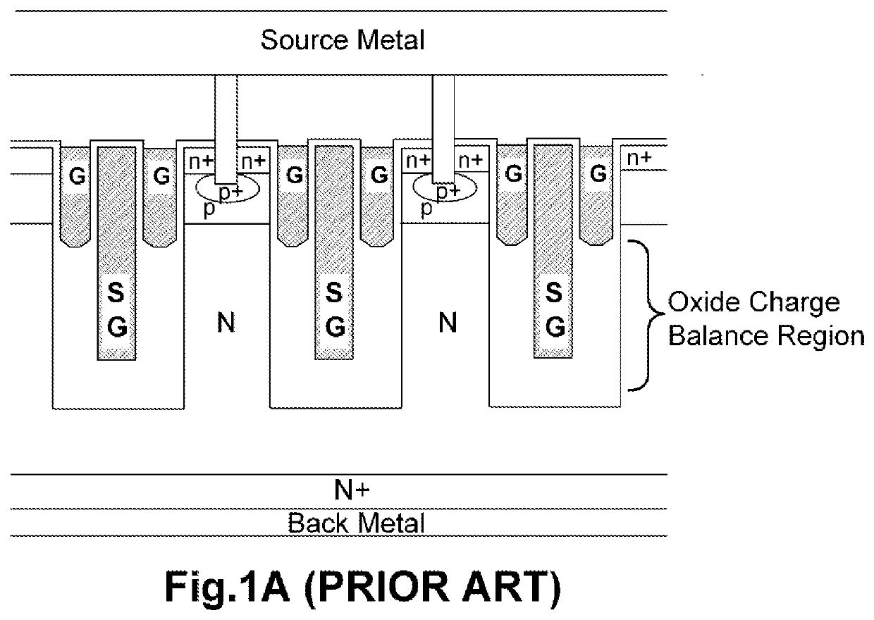
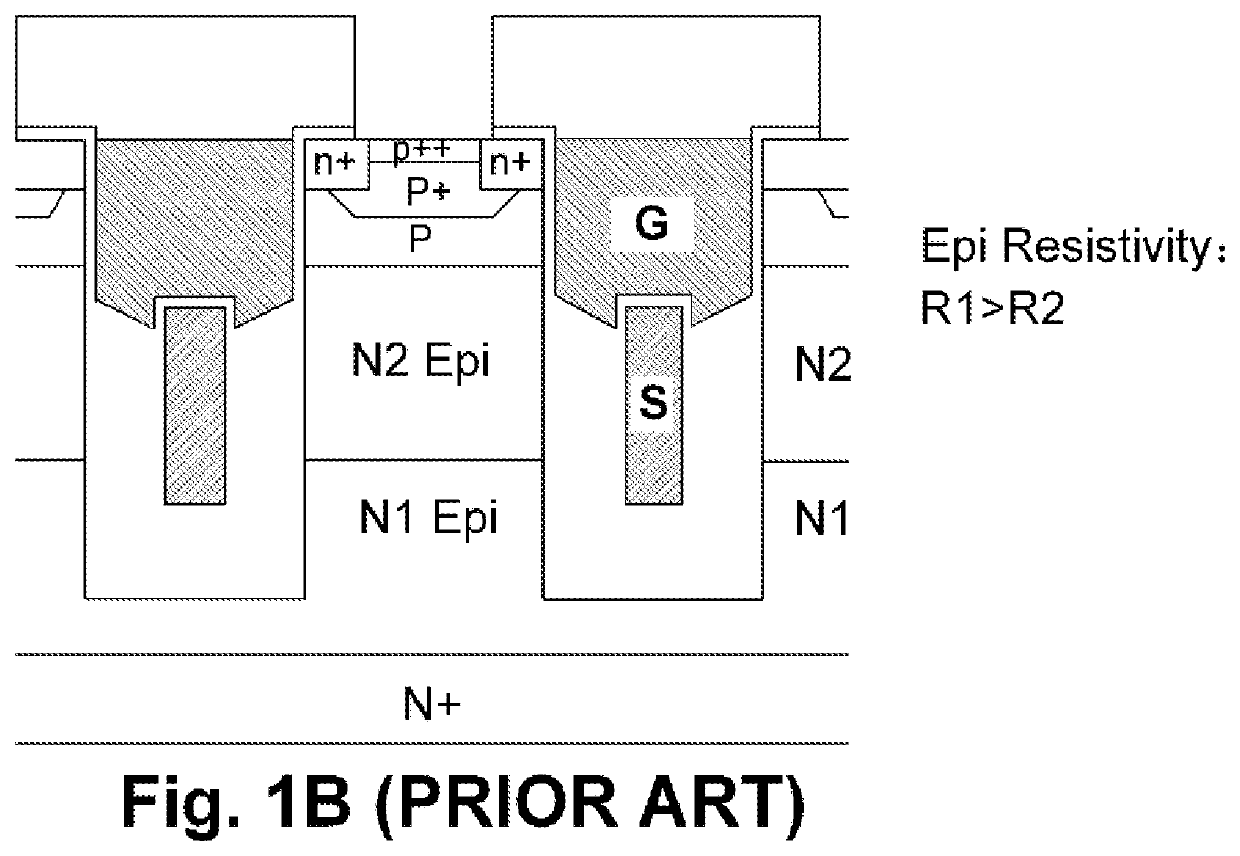
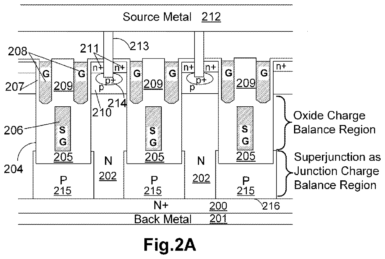
[0031]In the following Detailed Description, reference is made to the accompanying drawings, .which forms a part thereof, and in which is shown by way of illustration specific embodiments in which the invention may be practiced. In this regard, directional terminology, such as “top”, “bottom”, “front”, “back”, etc., is used with reference to the orientation of the Figure(s) being described. Because components of embodiments can be positioned in a number of different orientations, the directional terminology is used for purpose of illustration and is in no way limiting. It is to be understood that other embodiments may be utilized and structural or logical changes may be made without departing from the scope of the present invention. The following detailed description, therefore, is not to be taken in a limiting sense, and the scope of the present invention is defined by the appended claims. It is to be understood that the features of the various exemplary embodiments described herei...


PUM

PropertyMeasurementUnit
conductivityaaaaaaaaaa
charge balanceaaaaaaaaaa
thicknessaaaaaaaaaa

Abstract

A trenched semiconductor power device is disclosed comprising a plurality of trenched gates, each including a pair of split gate electrodes and a shielded gate electrode forming an oxide charge balance region between adjacent trenched gates, and junction charge balance region below trench bottom. The trenched semiconductor power device further comprises a super junction structure including a plurality of alternating P and N regions disposed above a substrate forming a junction charge balance region below the oxide charge balance region for breakdown voltage enhancement and on-resistance reductions.

Description

FIELD OF THE INVENTION[0001]This invention relates generally to semiconductor devices, and more particularly, to a super shielded gate trench MOSFET (Metal Oxide Semiconductor Field Effect Transistor) having oxide charge balance region between adjacent trenched gates and junction charge balance region below trench bottom to maintain a stable high breakdown voltage and lower on-resistance.BACKGROUND OF THE INVENTION[0002]Shielded gate trench MOSFETs (SGT) as shown in FIG. 1A have much lower gate charge and on-resistance compared with traditional single gate trench MOSFETs as results of existence of oxide charge balance region in drift region and thick oxide underneath gate electrode. However, an early breakdown always occurs at trench bottom. A degradation of the breakdown voltage is therefore becoming a design and operation limitation.[0003]To improve the early breakdown issue, U.S. Pat. No. 8,159,021 disclosed a SGT MOSFET with double epitaxial layers having two different resistivi...

Claims


Application Information

Patent Timeline
Patent Type & Authority Applications(United States)
IPC IPC(8): H01L29/78H01L29/06H01L29/10H01L29/40H01L21/02H01L21/265H01L21/765H01L29/66
CPCH01L29/7813H01L29/0634H01L29/1095H01L29/407H01L29/66734H01L21/02532H01L21/02579H01L21/26513H01L21/765H01L29/408H01L29/78H01L29/66477H01L29/0603H01L29/0684H01L29/4236H01L29/0623H01L29/41766H01L29/0878H01L29/7397H01L29/0834
Inventor HSIEH, FU-YUAN
Owner NAMI MOS CO LTD
Why Eureka
Try Eureka