Silicon carbide MOSFET device with avalanche charge transition buffer layer and preparation method of silicon carbide MOSFET device

A buffer layer and silicon carbide technology, which is applied in semiconductor/solid-state device manufacturing, electrical components, semiconductor devices, etc., can solve problems such as device failure and local temperature rise, so as to slow down local temperature rise, improve avalanche capability, and enhance avalanche reliability effect

Inactive Publication Date: 2021-08-27
UNIV OF ELECTRONICS SCI & TECH OF CHINA
View PDF19 Cites 3 Cited by
  • Summary
  • Abstract
  • Description
  • Claims
  • Application Information

AI Technical Summary

Problems solved by technology

After the avalanche of the device occurs, a large amount of avalanche charges will be discharged through the corner of the P-type base region under the action of a strong electric field. fail

Method used


Image

  • Silicon carbide MOSFET device with avalanche charge transition buffer layer and preparation method of silicon carbide MOSFET device
  • Silicon carbide MOSFET device with avalanche charge transition buffer layer and preparation method of silicon carbide MOSFET device
  • Silicon carbide MOSFET device with avalanche charge transition buffer layer and preparation method of silicon carbide MOSFET device

Examples


Embodiment 1

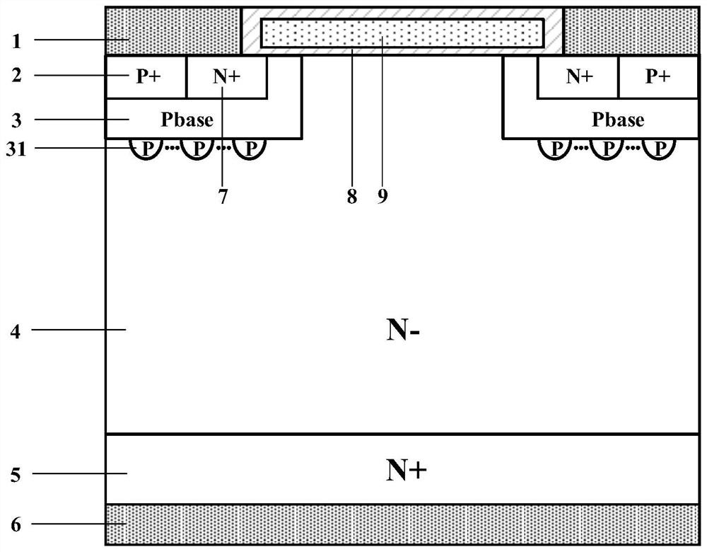
[0036] like figure 1 As shown, a silicon carbide MOSFET device with an avalanche charge transition buffer layer includes a drain metal 6, an N+ substrate 5 above the drain metal 6, and an N-drift region 4 above the N+ substrate 5; the N - There is a gate dielectric 8 and a polysilicon gate 9 in the middle of the upper part of the drift region 4; a P-type base region 3 is respectively arranged on the upper left and upper right inside the N-drift region 4, and the P-type base region 3 is below the P-type avalanche charge Transition buffer layer 31; the upper left P-type base region 3 includes the upper left P+ ohmic contact region 2, the N+ source region 7 on the right side of the P+ ohmic contact region 2; the upper right P-type base region 3 includes the upper right The P+ ohmic contact region 2, the N+ source region 7 on the left side of the P+ ohmic contact region 2; the source metal 1 above the N+ source region 7 and the P+ ohmic contact region 2; the part of the P-type bas...

Embodiment 2

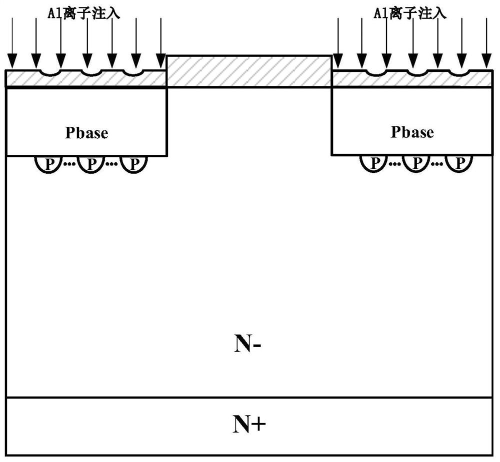
[0043] like Figure 2-Figure 9 As shown, the present embodiment provides a method for preparing the aforementioned silicon carbide MOSFET device having an avalanche charge transition buffer layer, comprising the following steps:

[0044] The first step: cleaning the epitaxial wafer, N-epitaxial with SiO 2 Implanting aluminum ions into the injection barrier layer to form a P-type avalanche charge transition buffer layer and a P-type base region;

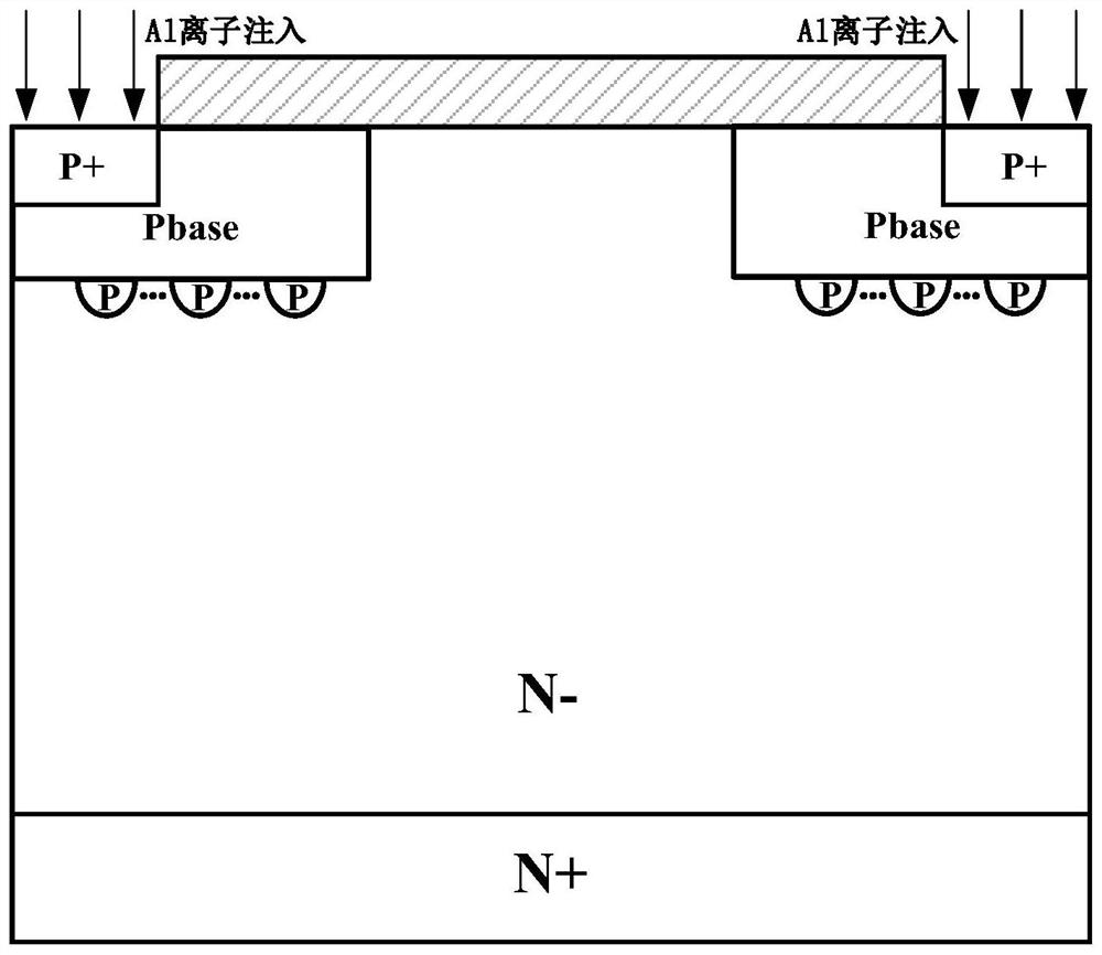
[0045] Step 2: Implant aluminum ions to form P+ ohmic contact area;

[0046]Step 3: Implant nitrogen ions to form N+ source region and activate annealing;

[0047] The fourth step: wet oxygen oxidation to form a gate oxide layer;

[0048] Step 5: Deposit polysilicon, anneal after ion implantation and pattern the polysilicon;

[0049] Step 6: Deposit gate metal to form gate electrode;

[0050] Step 7: thermally grow the isolation oxide layer;

[0051] Step 8: Etching SiO 2 , depositing a source metal to form a source electrode; ...


PUM


Abstract

The invention provides a silicon carbide MOSFET device with an avalanche charge transition buffer layer and a manufacturing method of the silicon carbide MOSFET device, and the method comprises the steps: injecting aluminum ions into an N-epitaxial layer, forming a P-type avalanche charge transition buffer layer and a P-type base region at the same time, and adjusting the injection depth through the thickness of a SiO2 mask; injecting aluminum ions to form a P + ohmic contact region; performing nitrogen ion implantation to form an N + source region and activating annealing; performing thermal growth and nitriding annealing on the gate oxide layer; depositing and etching polycrystalline silicon; introducing a plurality of electric field peak values below the P-type base region through the P-type avalanche charge transition buffer layer, after avalanche occurs on the device, and discharging avalanche charges from the P-type avalanche charge transition buffer layer and the corner of the P-type base region, so the generated current is in discrete distribution, the increase of local temperature is greatly alleviated, the avalanche capability of the device is improved, and the avalanche reliability of the silicon carbide MOSFET device in the blocking state is successfully enhanced.

Description

technical field [0001] The invention belongs to the technical field of power semiconductors, in particular to a silicon carbide MOSFET device with an avalanche charge transition buffer layer. Background technique [0002] Silicon carbide (Silicon Carbide) material, as one of the representatives of the third generation wide bandgap semiconductor materials, has a high breakdown electric field strength (4×10 6 V / cm), high carrier saturation drift velocity (2×10 7 cm / s), high thermal conductivity (490W / m·k), and good thermal stability make it have broad application prospects in the fields of high-power, high-temperature and high-frequency power electronics. [0003] MOSFET is one of the most widely used devices in silicon carbide power devices. Compared with bipolar devices, silicon carbide MOSFET has lower switching loss and higher frequency characteristics because it has no charge storage effect. As a voltage-type control device, power MOSFET has been widely used in power el...

Claims


Application Information

Patent Timeline
Patent Type & Authority Applications(China)
IPC IPC(8): H01L29/78H01L29/06H01L21/04
CPCH01L29/7802H01L29/0619H01L21/0445H01L29/66068
Inventor 李轩叶俊杰吴阳阳王常旺邓小川张波
Owner UNIV OF ELECTRONICS SCI & TECH OF CHINA
Why Eureka
Try Eureka