Semiconductor device having a variation lateral doping structure and method for manufaturing the same

a technology of lateral doping structure and semiconductor device, which is applied in the direction of semiconductor device, electrical apparatus, transistor, etc., can solve the problems of broken p-type base layer provided between the gate pad and the cell region, and achieve the effect of improving the avalanche capacity

Active Publication Date: 2015-07-28
MITSUBISHI ELECTRIC CORP
View PDF6 Cites 2 Cited by
  • Summary
  • Abstract
  • Description
  • Claims
  • Application Information

AI Technical Summary

Benefits of technology

[0007]In view of the above-described problems, an object of the present invention is to provide a semiconductor device that can improve avalanche capacity without generating breakdown voltage lowering or ON resistance increasing, and a method for manufacturing the same.
[0009]The present invention makes it possible to improve avalanche capacity without generating breakdown voltage lowering or ON resistance increasing.

Problems solved by technology

If the avalanche current can easily flow to places other than the cell region due to the improvement of breakdown voltage of the cell region, there was a problem wherein the P-type base layers provided between the gate pad and the cell region are broken due to the concentration of currents in the avalanche operation.

Method used


Image

  • Semiconductor device having a variation lateral doping structure and method for manufaturing the same
  • Semiconductor device having a variation lateral doping structure and method for manufaturing the same
  • Semiconductor device having a variation lateral doping structure and method for manufaturing the same

Examples


first embodiment

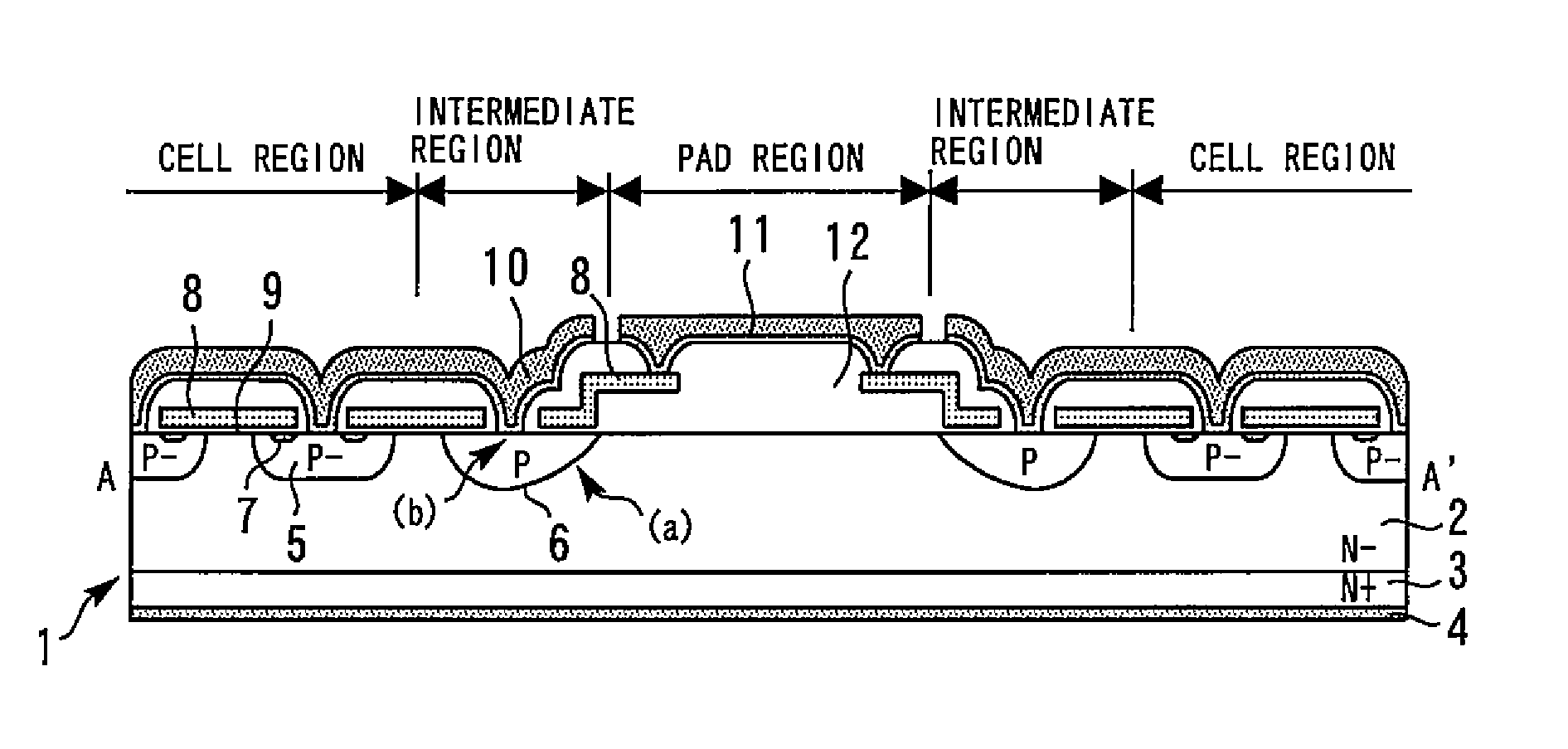
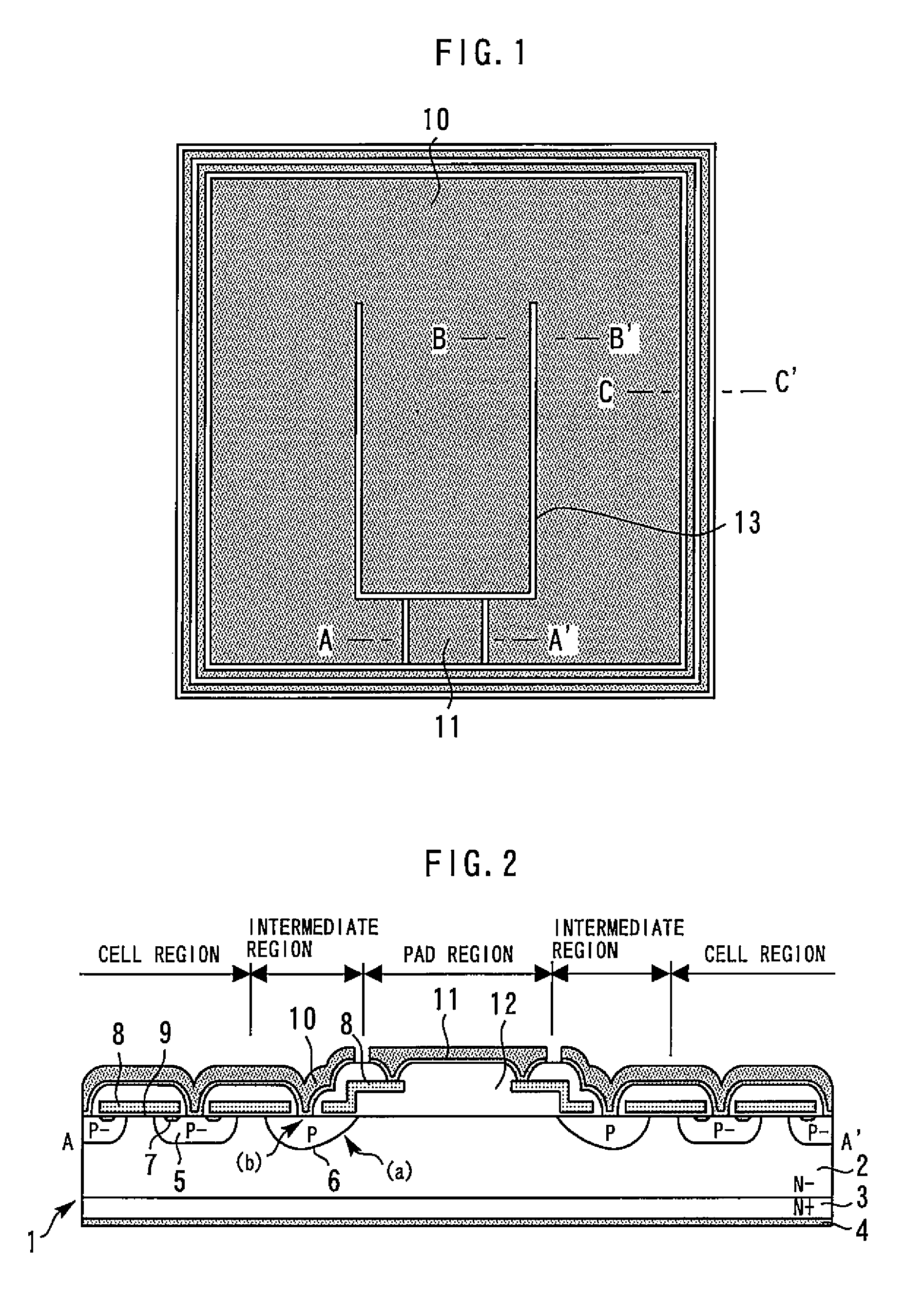
[0028]FIG. 1 is a top view showing a semiconductor device according to the first embodiment of the present invention. FIG. 2 is a sectional view taken along the line A-A′ in FIG. 1.

[0029]A silicon substrate 1 has a cell region, a pad region, an intermediate region, and an edge termination region. The intermediate region is placed between the cell region and the pad region. The edge termination region is placed outside the cell region and the pad region.

[0030]An N−-type drain layer 2 is provided on the entire region in the silicon substrate 1. An N+-type drain layer 3 is provided under the N−-type drain layer 2, and a drain electrode 4 is connected on the lower face of the N+-type drain layer 3.

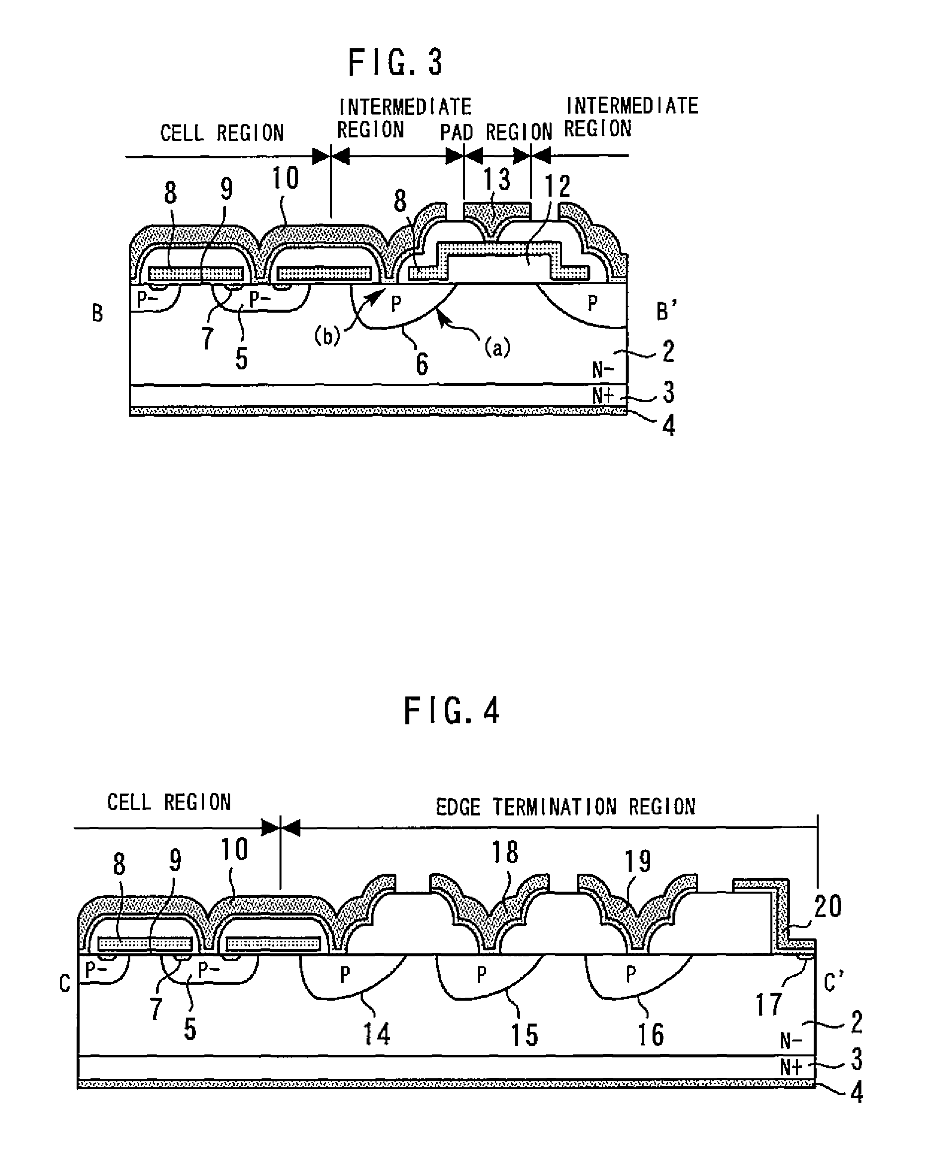
[0031]In the cell region, a P−-type base layer 5 is provided on the N−-type drain layer 2. In the intermediate region, a P-type base layer 6 is provided on the N−-type drain layer 2. In the P−-type base layer 5, an N+-type source region 7 is provided. A gate electrode 8 is provided on a channe...

second embodiment

[0050]FIG. 16 is a sectional view showing a semiconductor device according to the second embodiment of the present invention. In addition to the configuration of the first embodiment, a P-type base layer 23 is provided on the N−-type drain layer 2 in the pad region. The P-type base layer 6 in the intermediate region is connected to the P-type base layer 23 in the pad region. However, different from the first comparative example, the P-type base layer 23 is shallower than the deepest portion of the P-type base layer 6.

[0051]FIG. 17 is the graphs showing the field strength under the gate pad in the second embodiment and the first comparative example. The abscissas show the field strengths, and the ordinates show the depths from the surface of the silicon substrate 1. The areas of the triangles in the graphs correspond to the voltages maintained by the N−-type drain layer 2 and the P-type base layer 23, respectively. In the first comparative example, almost all breakdown voltage is mai...

third embodiment

[0056]FIG. 19 is a sectional view showing a semiconductor device according to the third embodiment of the present invention. In place of the P-type base layers 6 of the first embodiment, the P-type base layers 24 are provided on the N−-type drain layer 2 in the intermediate region and the pad region. The impurity concentration in the P-type base layers 24 increases toward the center of the gate pad 11, and reaches the peak at the center portion of the gate pad 11. The impurity concentration gradation of the P-type base layers 24 has a more gentle VLD structure in comparison with the P-type base layers 5. Thereby, the impact-ionized current in the avalanche operation can be lowered.

[0057]In addition, in the first to third embodiments, the present invention is applied to the n-channel power MOSFET. However, the present invention is not limited to this application and can also be applied to p-channel power MOSFETs, IGBTs, or SiC devices.


PUM


Abstract

A semiconductor device including a semiconductor layer of a first conductivity type in a cell region, a first base layer of a second conductivity type on the semiconductor layer in the cell region; a second base layer of the second conductivity type on the semiconductor layer in an intermediate region; a conductive region of a first conductivity type in the first base layer; a gate electrode on a channel region placed between the conductive region and the semiconductor layer; a first electrode connected to the first and second base layers; a second electrode connected to the semiconductor layer; and a gate pad on the semiconductor layer via an insulating film in a pad region and connected to the gate electrode, an impurity concentration gradation in the gate pad side of the second base layer has a gentler VLD structure than an impurity concentration gradation in the first base layer.

Description

BACKGROUND OF THE INVENTION[0001]1. Field of the Invention[0002]The present invention relates to a semiconductor device that can improve avalanche capacity without generating breakdown voltage lowering or ON resistance increasing, and a method for manufacturing the same.[0003]2. Background Art[0004]In order to realize the demands of markets, such as energy saving and device downsizing, the low loss of the transient state in the ON state and switching in semiconductor devices such as MOSFET and IGBT is demanded. Here, if only the ON state is observed, low loss can be enabled by making the wafer specification in the epitaxial layer which is a bulk portion have low resistance to lower the ON resistance. However, the ON resistance and the breakdown voltage are in the trade-off relation, and by simply making the wafer specification have a low resistance, the breakdown voltage of the element is lowered, and the object cannot be achieved. Therefore, by obtaining the effect of ON-resistance...

Claims


Application Information

Patent Timeline
Patent Type & Authority Patents(United States)
IPC IPC(8): H01L29/66H01L29/739H01L29/10H01L21/266H01L21/225H01L29/78H01L29/36H01L29/06H01L29/423
CPCH01L29/1095H01L21/2253H01L21/266H01L29/0615H01L29/0619H01L29/66333H01L29/66712H01L29/7395H01L29/7802H01L29/7811H01L29/06H01L29/0638H01L29/0696H01L29/36H01L29/42372H01L29/7834
Inventor TAKANO, KAZUTOYO
Owner MITSUBISHI ELECTRIC CORP
Why Eureka
Try Eureka