

Semiconductor device
a technology of semiconductors and devices, applied in the direction of semiconductor devices, electrical devices, transistors, etc., can solve the problems of increasing gate resistance, and achieve the effect of improving avalanche capability and reducing on-state resistan
- Summary
- Abstract
- Description
- Claims
- Application Information
AI Technical Summary
Benefits of technology
Problems solved by technology
Method used
Image

Examples
first embodiment
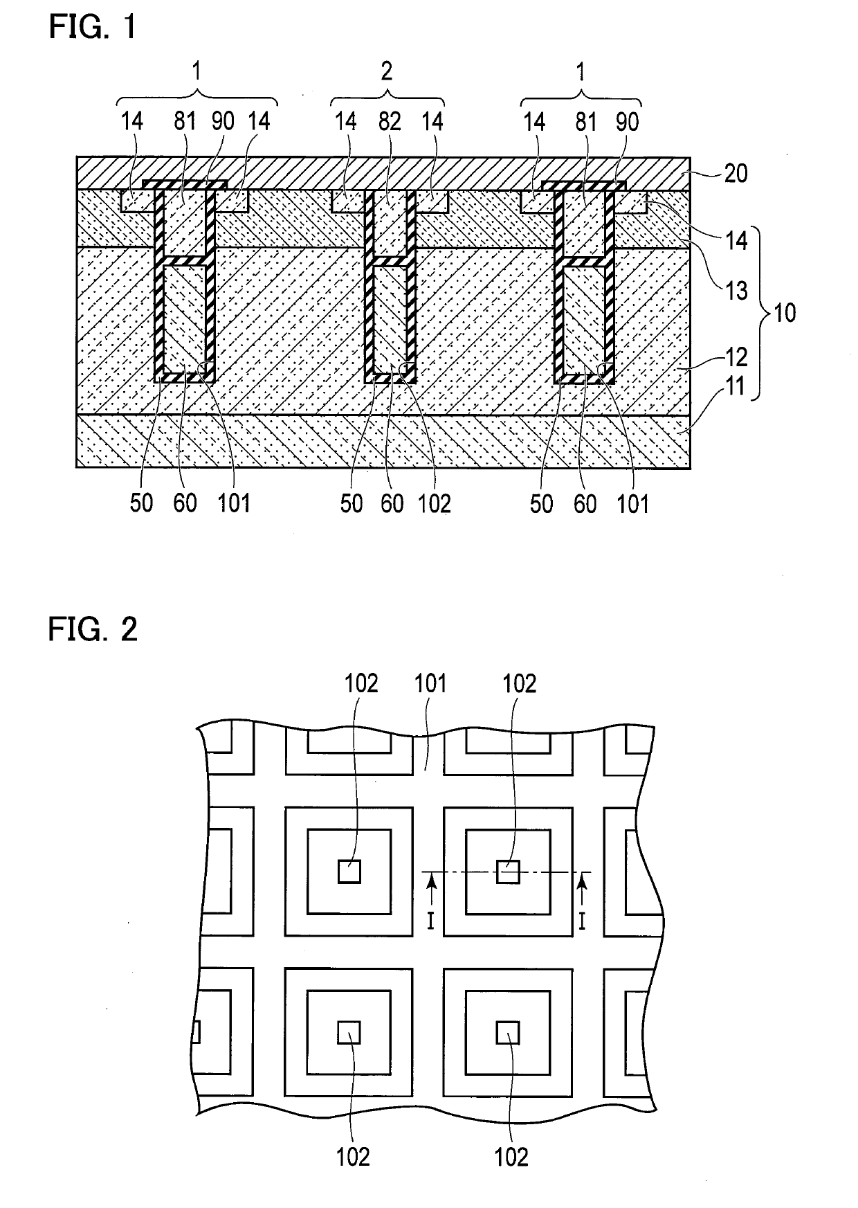
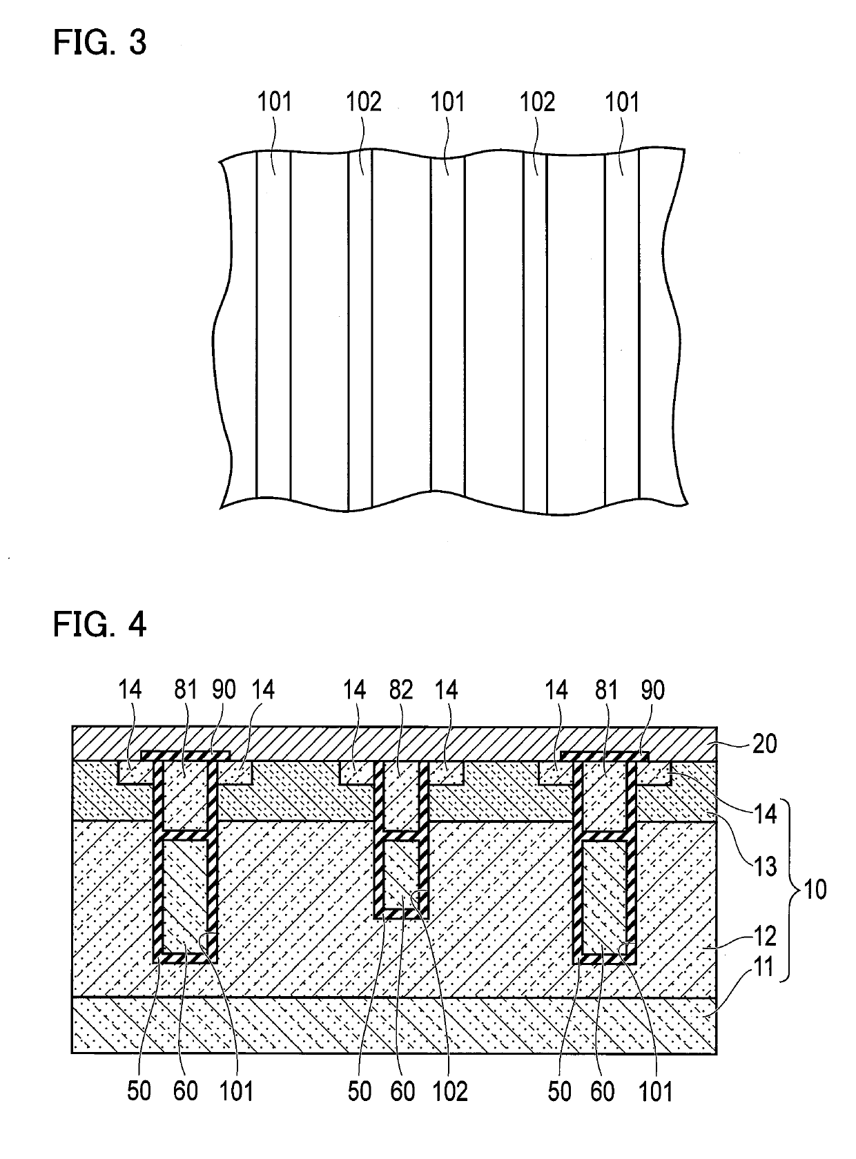
[0019]As illustrated in FIG. 1, a semiconductor device according to a first embodiment of the present invention includes a first semiconductor element 1 and second semiconductor elements 2 formed in a semiconductor base 10. The first semiconductor element 1 includes a first gate electrode 81 provided within a first trench 101 formed in the semiconductor base 10. The second semiconductor elements 2 includes a second gate electrode 82 provided within a second trench 102 formed in the semiconductor base 10. As illustrated in FIG. 2, the first trench 101 has a mesh-like shape in a plan view while the second trenches 102, which are columnar, are formed in mesh openings surrounded by the first trench 101. As illustrated in FIG. 2, the second trenches 102, which are rectangular in a plan view, are formed in the respective plural mesh openings. FIG. 1 is a cross-sectional view in a I-I direction of FIG. 2.
[0020]The semiconductor base 10 includes: an n-type drain region 12 provided on an n-t...
second embodiment
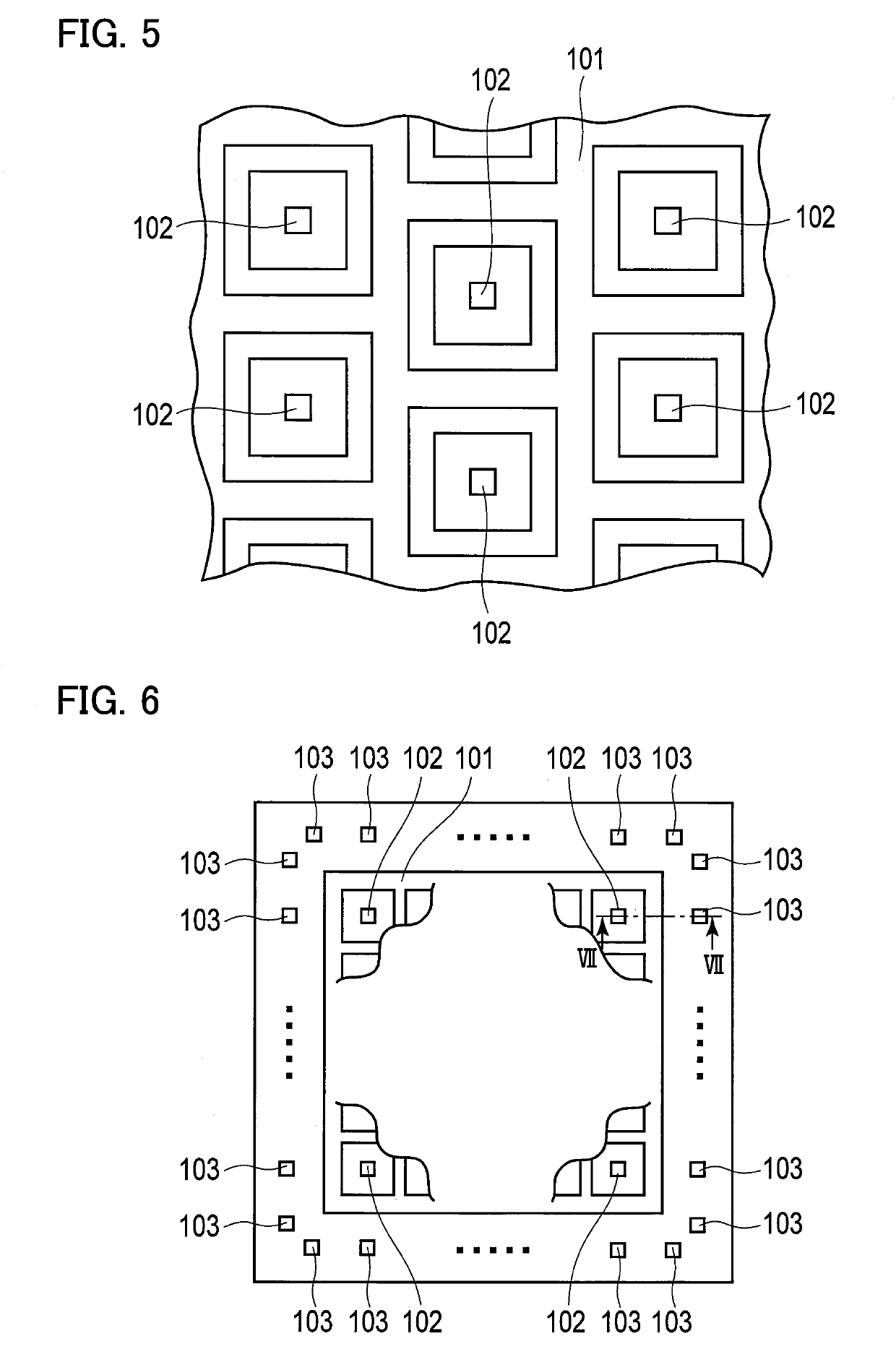
[0033]As illustrated in FIG. 6, a semiconductor device according to a second embodiment of the present invention is different from that in FIG. 2 in that third trenches 103 are formed in the periphery of the semiconductor base 10 outside the first trench 101. The other configuration thereof is the same as that of the first embodiment.
[0034]In the semiconductor device illustrated in FIG. 6, the plural third trenches 103, which are columnar, are arranged in the periphery of the semiconductor base 10 so as to separate from each other. FIG. 7 illustrates a cross-sectional view along a VII-VII direction of FIG. 6.
[0035]As illustrated in FIG. 7, a third gate electrode 83 is provided within each third trench 103, and third semiconductor elements 3 are formed in the periphery of the semiconductor base 10. The third semiconductor elements 3 are MOS diodes of the same structure as that of the second semiconductor elements 2. Specifically, each third trench 103 extends from the upper surface o...
first modification
[0041]FIG. 8 illustrates a semiconductor device according to a first modification of the second embodiment of the present invention. In the semiconductor device illustrated in FIG. 8, the third trenches 103 may include a third trench 103 which is formed in an annular shape in a plan view in the periphery of the semiconductor base 10 so as to surround the circumference of the first trench 101. In such a manner, the third trenches 103, which are provided outside the first trench 101, do not need to be columnar as illustrated in FIG. 6.
[0042]In the example of the semiconductor device illustrated in FIG. 8, the single third trench 103 surrounds the circumference of the first trench 101. However, the third trench 103 may include plural annular third trenches 103. For example, the plural third trenches 103 include two or three third trenches 103 that surround the circumference of the first trench 101.
PUM
 Abstract
Description
Claims
Application Information