
Semiconductor light-emitting device

a technology of semiconductor light-emitting device and light-emitting diode, which is applied in the direction of semiconductor devices, basic electric elements, electrical appliances, etc., can solve the problems of poor brightness enhancement effect of light-emitting diodes, and achieve the effects of improving the light-emitting efficiency of semiconductor light-emitting devices, and improving the light-emitting efficiency of semiconductor light-

Active Publication Date: 2021-10-28
KAISTAR LIGHTING (XIAMEN) CO LTD
View PDF7 Cites 0 Cited by
  • Summary
  • Abstract
  • Description
  • Claims
  • Application Information

AI Technical Summary

Benefits of technology

The patent text describes a semiconductor light-emitting device that improves current spreading and increases light-emitting efficiency. This is achieved by forming multiple first convex structures on the side of the device near the second electrode, which helps to avoid excessive current concentration and allows for even distribution of radiation. Additionally, an adhesion enhancement layer is placed in direct contact with the aluminum layer of the first electrode, which further improves the device's light-emitting efficiency.

Problems solved by technology

However, the conventional light-emitting diode has an area where the current is too concentrated, resulting in a poor brightness enhancement effect of the light-emitting diode.

Method used


Image

  • Semiconductor light-emitting device
  • Semiconductor light-emitting device
  • Semiconductor light-emitting device

Examples


first embodiment

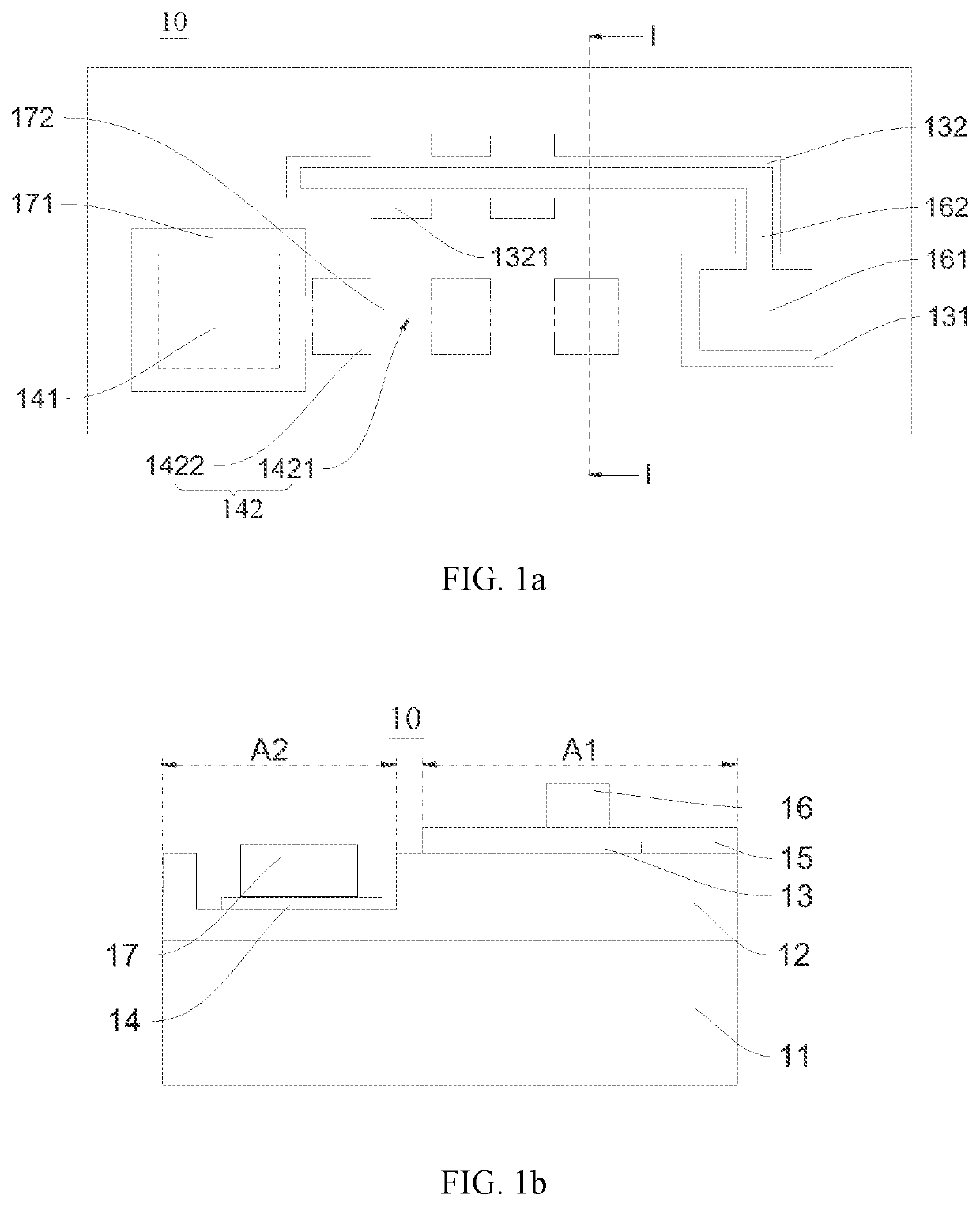
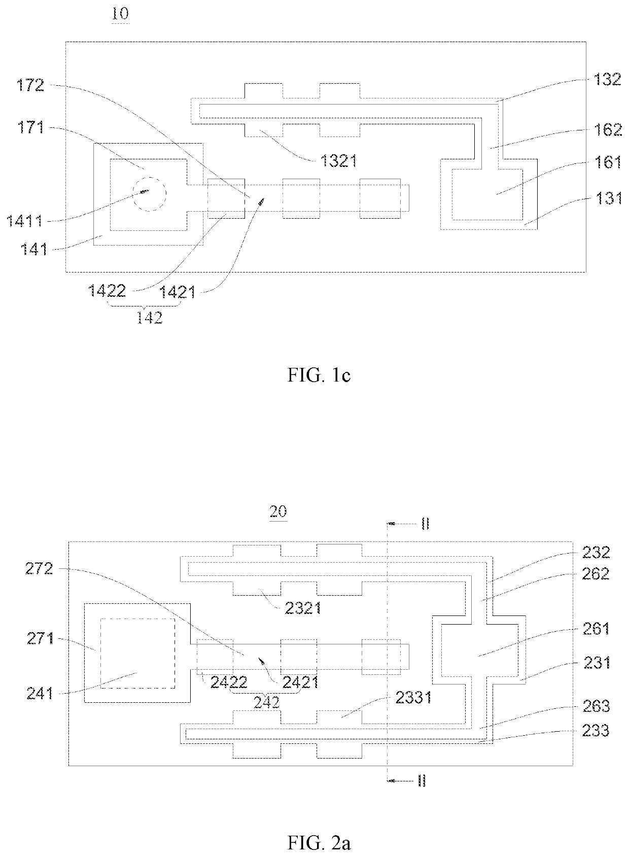
[0027]Referring to FIG. 1a and FIG. 1b, the first embodiment of the disclosure provides a semiconductor light-emitting device 10 such as a light-emitting diode (LED). As illustrated in FIG. 1a and FIG. 1b, the semiconductor light-emitting device 10 exemplarily includes: a substrate 11, an epitaxial layer structure 12, a current blocking layer 13, another current blocking layer 14, a current spreading layer 15, an electrode 16 and another electrode 17.

[0028]In particular, as shown in FIG. 1b, the epitaxial layer structure 12 is disposed on the substrate 11 and includes an area A1 and another area A2. The current blocking layer 13 is disposed on the epitaxial layer structure 12 and located in the area A1. The current blocking layer 14 is disposed on the epitaxial layer structure 12 and located in the area A2. The current spreading layer 15 is disposed on the epitaxial layer structure 12 and located in the area A1. The current spreading layer 15 covers the current blocking layer 13 and...

second embodiment

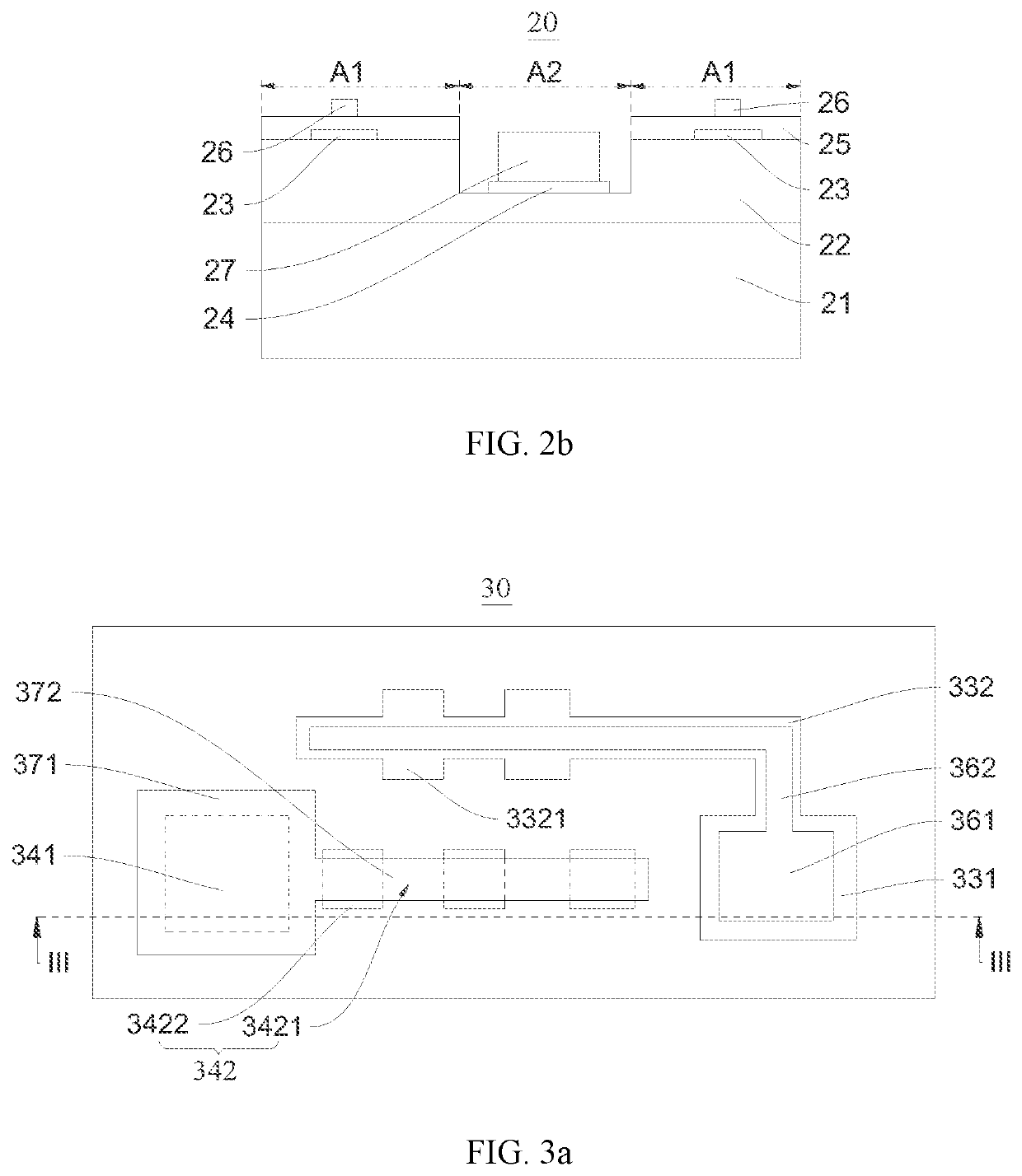
[0041]Referring to FIG. 2a and FIG. 2b, the second embodiment of the disclosure provides a semiconductor light-emitting device 20. As illustrated in FIG. 2a and FIG. 2b, the semiconductor light-emitting device 20 is similar to the semiconductor light-emitting device 10. The semiconductor light-emitting device 20 includes for example a substrate 21, an epitaxial layer structure 22, a current blocking layer 23, another current blocking layer 24, a current spreading layer 25, an electrode 26 and another electrode 27.

[0042]In particular, as shown in FIG. 2b, the epitaxial layer structure 22 is disposed on the substrate 21 and includes an area A1 and another area A2. The current blocking layer 23 is disposed on the epitaxial layer structure 22 and located in the area A1. The current blocking layer 24 is disposed on the epitaxial layer structure 22 and located in the area A2. The current spreading layer 25 is disposed on the epitaxial layer structure 22 and located in the area A1. The cur...

third embodiment

[0047]Referring to FIG. 3a and FIG. 3b, the third embodiment of the disclosure provides a semiconductor light-emitting device 30. As illustrated in FIG. 3a and FIG. 3b, the semiconductor light-emitting device 30 is similar to the semiconductor light-emitting device 10 and includes for example a substrate 31, an epitaxial layer structure 32, a current blocking layer 33, another current blocking layer 34, a current spreading layer 35, an electrode 36 and another electrode 37.

[0048]In particular, as shown in FIG. 3b, the epitaxial layer structure 32 is disposed on the substrate 31 and includes an area A1 and another area A2. The current blocking layer 33 is disposed on the epitaxial layer structure 32 and located in the area A1. The current blocking layer 34 is disposed on the epitaxial layer structure 32 and located in the area A2. The current spreading layer 35 is disposed on the epitaxial layer structure 32 and located in the area A1. The current spreading layer 35 covers the curren...


PUM

PropertyMeasurementUnit
light transmittanceaaaaaaaaaa
structureaaaaaaaaaa
widthaaaaaaaaaa

Abstract

A semiconductor light-emitting device includes: a substrate, an epitaxial layer structure disposed on the substrate, a first current blocking layer disposed on the epitaxial layer structure, a second current blocking layer disposed on the epitaxial layer structure, a current spreading layer disposed on the epitaxial layer structure and covering the first current blocking layer; a first electrode disposed on a side of the current spreading layer facing away from the epitaxial layer structure, and a second electrode disposed on the epitaxial layer structure and covering the second current blocking layer. The first current blocking layer includes a first main blocking portion and a first extended blocking portion. The second current blocking layer includes a second main blocking portion and a second extended blocking portion. The second extended blocking portion includes spacings. The first extended blocking portion is formed with convex structures. The convex structures are aligned with the spacings.

Description

FIELD OF THE DISCLOSURE[0001]The disclosure relates to the field of semiconductor technologies, and more particularly to a semiconductor light-emitting device.BACKGROUND OF THE DISCLOSURE[0002]With the continuous development of LED industries, cost-effective advantages of LED products are becoming increasingly prominent. A conventional light-emitting diode (LED) is provided with a current blocking layer under a P-type electrode to block a current passing therethrough. That is, when the current is introduced by the P-type electrode, the current blocking layer can block the current passing therethrough, thereby forcing the current to bypass the current blocking layer and be spread out by a transparent conductive layer, so that brightness of the light emitting diode is improved consequently. However, the conventional light-emitting diode has an area where the current is too concentrated, resulting in a poor brightness enhancement effect of the light-emitting diode.SUMMARY OF THE DISCLO...

Claims


Application Information

Patent Timeline
Patent Type & Authority Applications(United States)
IPC IPC(8): H01L33/14H01L33/38H01L33/40
CPCH01L33/145H01L33/40H01L33/38H01L33/44
Inventor LU, TSUNG-HONG
Owner KAISTAR LIGHTING (XIAMEN) CO LTD
Learn More