Conductive material using carbon nano-tube, and manufacturing method thereof

a technology of carbon nanotubes and conductive materials, which is applied in the direction of carbon-silicon compound conductors, electrolytic capacitors, cell components, etc., can solve the problems of low electric conductivity of activated carbon of great specific surface area, failure to deliver great current, and the increase capacity achieved by this method is still limited to about 1.7 times the conventional level, and achieve excellent corrosion resistance to acids. excellent

Inactive Publication Date: 2005-04-21
HITACHI ZOSEN CORP +1
View PDF6 Cites 71 Cited by
  • Summary
  • Abstract
  • Description
  • Claims
  • Application Information

AI Technical Summary

Benefits of technology

[0029] The conductive film may be a polyethylene film which is given electric conductivity by incorporating therein about 1 to about 30 wt. % of carbon nanotube pieces. The conductive carbon nanotube material obtained with use of the film incorporating carbon nanotube pieces has the advantage of being excellent in corrosion resistance to acids and alkalis because the conductive film is free from ITO (Indium Tin Oxide) and metals such as Ag and Cu. The conductive film may be a porous conductive film comprising a polyethylene layer having a metal layer, for example, of ITO, Ag, Cu or the like on the transfer surface and provided with numerous through holes. The conductive carbon nanotube material obtained with use of the porous conductive film readily permits diffusion of gases, exhibiting outstanding characteristics when used as an environment cleaning catalyst material. The conductive film may be a film having numerous through holes formed therein and comprising a polyethylene film which is given electric conductivity by incorporating therein about 1 to about 30 wt. % of carbon nanotube pieces. The conductive carbon nanotube material obtained with use of this porous conductive film readily permits diffusion of gases, exhibiting outstanding characteristics when used as an environment cleaning catalyst material, and has the advantage of being excellent in corrosion resistance to acids and alkalis because the conductive film is free from ITO and metals such as Ag and Cu.

Problems solved by technology

However, activated carbon of great specific surface area is generally low in electric conductivity, and the use of activated carbon only imparts increased internal resistance to the polarizable electrode, which in turn fails to deliver great current.
The increased capacity achieved by this method is nevertheless limited to about 1.7 times the conventional level.
The conventional electric double layer capacitor further requires a separator of PTFE or the like to completely prevent ohmic contact between the positive and negative electrodes and not to impede the passage of ions, whereas the capacitor has the problem that the material and shape of the separator exert a great influence on the self-discharge characteristics and internal resistance of the electric double layer.
However, the invention uses the chemical vapor deposition process (CVD process) in an atmosphere of at least 600° C. for producing carbon nanotube electrodes, so that the process requires use of a substrate of metal, glass or like heat-resistant material, which therefore results in a high product cost.
Thus, the process has the problem of being unsuited to quantity production.

Method used


Image

  • Conductive material using carbon nano-tube, and manufacturing method thereof
  • Conductive material using carbon nano-tube, and manufacturing method thereof
  • Conductive material using carbon nano-tube, and manufacturing method thereof

Examples


example 1

[First Step]

[0037] A solution of Fe complex was splayed onto a low-resistance N-type semiconductor silicon substrate, 0.5 mm in thickness, and the substrate was heated at 220° C. to form an iron coating.

[Second Step]

[0038] The iron coating on the substrate was placed into a CVD apparatus. Acetylene serving as a material for carbon nanotubes was introduced into the CVD apparatus at a flow rate of 30 ml / min at a temperature of about 720° C. for 15 minutes. When thus heated, the iron coating was made into particles, and bristle-like carbon nanotubes were produced and gradually grown, with the resulting catalyst particles serving as nuclei. The carbon nanotubes grown had a multilayer structure and were 12 nm in thickness and 50 μm in length.

[Third Step]

[0039] The bristle-like carbon nanotubes obtained were pressed at their outer ends against a conductive film (CF48, product of Toray Industries, Inc.) having a thickness of 0.2 mm and heated to a temperature not lower than the soften...

example 2

[0041] This example shows a process for producing a carbon nanotube electrode by performing the steps of Example 1 continuously.
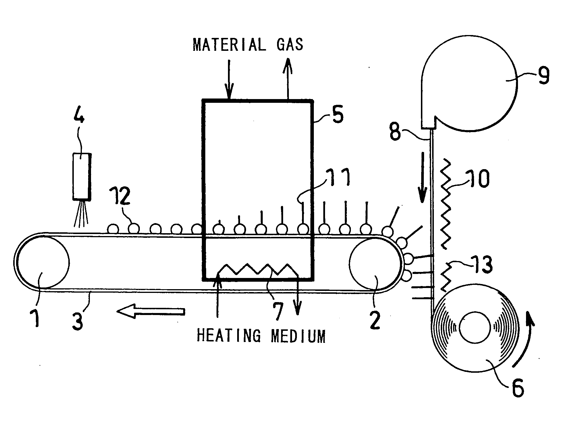
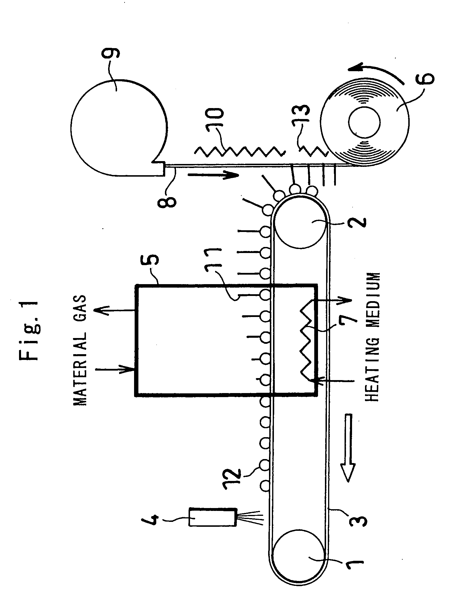
[First Step]

[0042]FIG. 1 shows an endless belt 3 (comprising a low-resistance N-type silicon substrate having a thickness of 0.5 mm) which was driven at a feed speed of 12 m / h by a drive drum 1 and a driven drum 2. A solution of Fe complex was applied to the upper surface of the endless belt 3 by a spray 4 in a catalyst deposition zone at an upper-side upstream portion of the belt 3 and thereafter heated to 220° C., whereby catalyst particles 12 were formed as scattered at a spacing of 100 nm on the belt 3.

[Second Step]

[0043] The catalyst particles 12 on the endless belt 3 were transported to a CVD zone downstream from the catalyst deposition zone. The CVD zone comprised a heating furnace 5 having a length of about 2 m in the direction of movement of the belt, and a heater 7 disposed inside the furnace 5 under the belt 3. Acetylene gas serving as a mate...

example 3

[First Step]

[0046] The same procedure as in Example 1 was performed.

[Second Step]

[0047] The same procedure as in Example 1 was performed.

[Third Step]

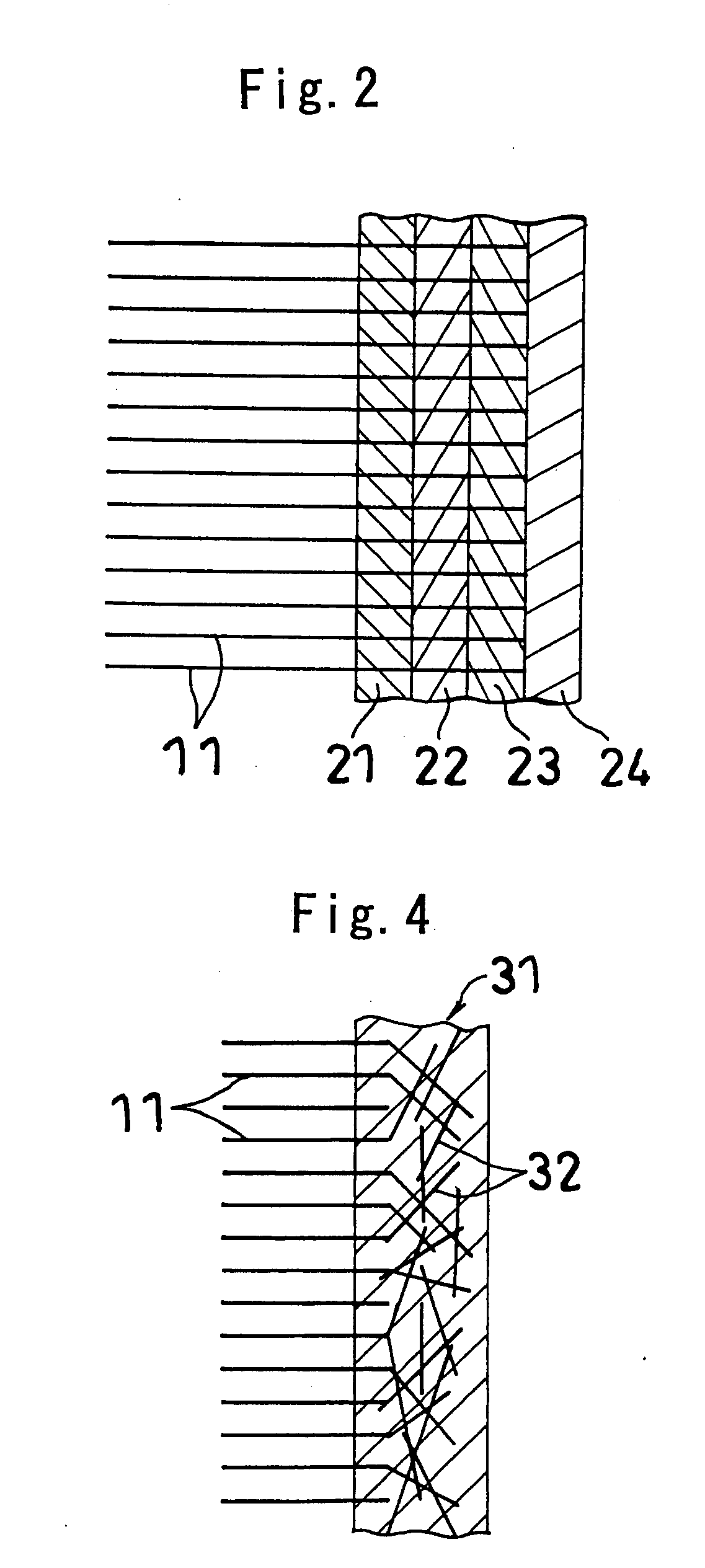
[0048] The bristle-like carbon nanotubes 11 formed on the 0.5-mm-thick low-resistance N-type semiconductor silicon substrate by the second step were pressed at their outer ends against a conductive multilayer film heated at 95° C., whereby the carbon nanotubes were implanted in the conductive film substantially perpendicular to the film surface. With reference to FIG. 2, the conductive multilayer film comprises, as arranged from the transfer side toward the other side, an ITO (Indium Tin Oxide) layer 21 having a thickness of 0.01 to 0.03 μm, a primer layer 22 having a thickness of 0.05 to 0.5 μm, a polyethylene layer 23 having a thickness of 20 to 50 μm and a polyethylene terephthalate layer 24 having a thickness of 50 to 180 μm. The polyethylene layer may comprise other heat-resistant film.

[Fourth Step]

[0049] The conductive film...


PUM

PropertyMeasurementUnit
temperatureaaaaaaaaaa
bore diameteraaaaaaaaaa

Abstract

An object of the invention is to provide a carbon nanotube electrode which is suited to quantity production and advantageous in cost, and a process for producing the same. When carbon nanotubes on respective catalyst particles 12 on an endless belt 3 gradually fall down to a horizontal position while moving around a driven drum 2 after traveling from a CVD zone to a transfer zone with the movement of the belt, the carbon nanotubes 11 have their outer ends pressed against a conductive film 8. The conductive film 8 is sent out from a film feeder 9 downward and heated by a heater 10 to a temperature not lower than the softening temperature of the film to below the melting temperature thereof. The carbon nanotubes 11 are transferred from the catalyst particles 12 to the conductive film 8 substantially perpendicular to the film surface by being pressed against the conductive film 8 in this way.

Description

TECHNICAL FIELD [0001] The present invention relates to an electrically conductive material comprising carbon nanotubes and a process for producing the same. The conductive material of the invention is usable, for example, for electrodes which are the main components of electric double layer capacitors having a great capacity to store electricity. The present invention further relates to an electrically conductive material comprising carbon nanotubes resembling elongated bristles of a brush and having high linearity and a great value as carbon nanotubes for use as fuel cell electrodes, environment cleaning catalytic materials, electron sources, electronic materials, probe explorers and gas storage materials, and a process for producing the material. BACKGROUND ART [0002] Conventional electric double layer capacitors include a capacitor element which comprises a pair of polarizable electrodes each prepared by forming a polarizable electrode layer mainly of activated carbon over a cur...

Claims


Application Information

Patent Timeline
Patent Type & Authority Applications(United States)
IPC IPC(8): B82Y30/00B82Y99/00C01B31/02H01B1/04H01B1/24H01B13/00H01G9/00H01G11/22H01G11/36H01G11/86H01M4/96
CPCB82Y30/00B82Y40/00C01B31/0233Y02E60/50H01G11/36H01M4/96Y02E60/13H01B1/24C01B32/162H01B1/04H01B13/00
Inventor NAKAYAMA, YOSHIKAZUINAZUMI, CHIKASHISHIOZAKI, HIDEKIFUJITA, DAISUKE
Owner HITACHI ZOSEN CORP
Why Eureka
Try Eureka