Semiconductor device and manufacturing method thereof

a semiconductor and semiconductor technology, applied in non-linear optics, instruments, optics, etc., can solve problems such as the difference between the stoichiometric composition of an oxide semiconductor and the stoichiometric composition, and achieve the effect of easy breakag

Active Publication Date: 2011-04-07
SEMICON ENERGY LAB CO LTD
View PDF112 Cites 73 Cited by
  • Summary
  • Abstract
  • Description
  • Claims
  • Application Information

AI Technical Summary

Benefits of technology

[0029]Since a thin film transistor is easily broken due to static electricity or the like, a protective circuit for protecting the thin film transistor in the pixel portion is preferably provided over the same substrate for a gate line or a source line. The protective circuit is preferably formed using a non-linear element including an oxide semiconductor layer.

Problems solved by technology

However, a difference from the stoichiometric composition in an oxide semiconductor arises in a thin film formation process.

Method used


Image

  • Semiconductor device and manufacturing method thereof
  • Semiconductor device and manufacturing method thereof
  • Semiconductor device and manufacturing method thereof

Examples


embodiment 1

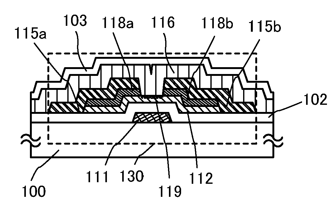
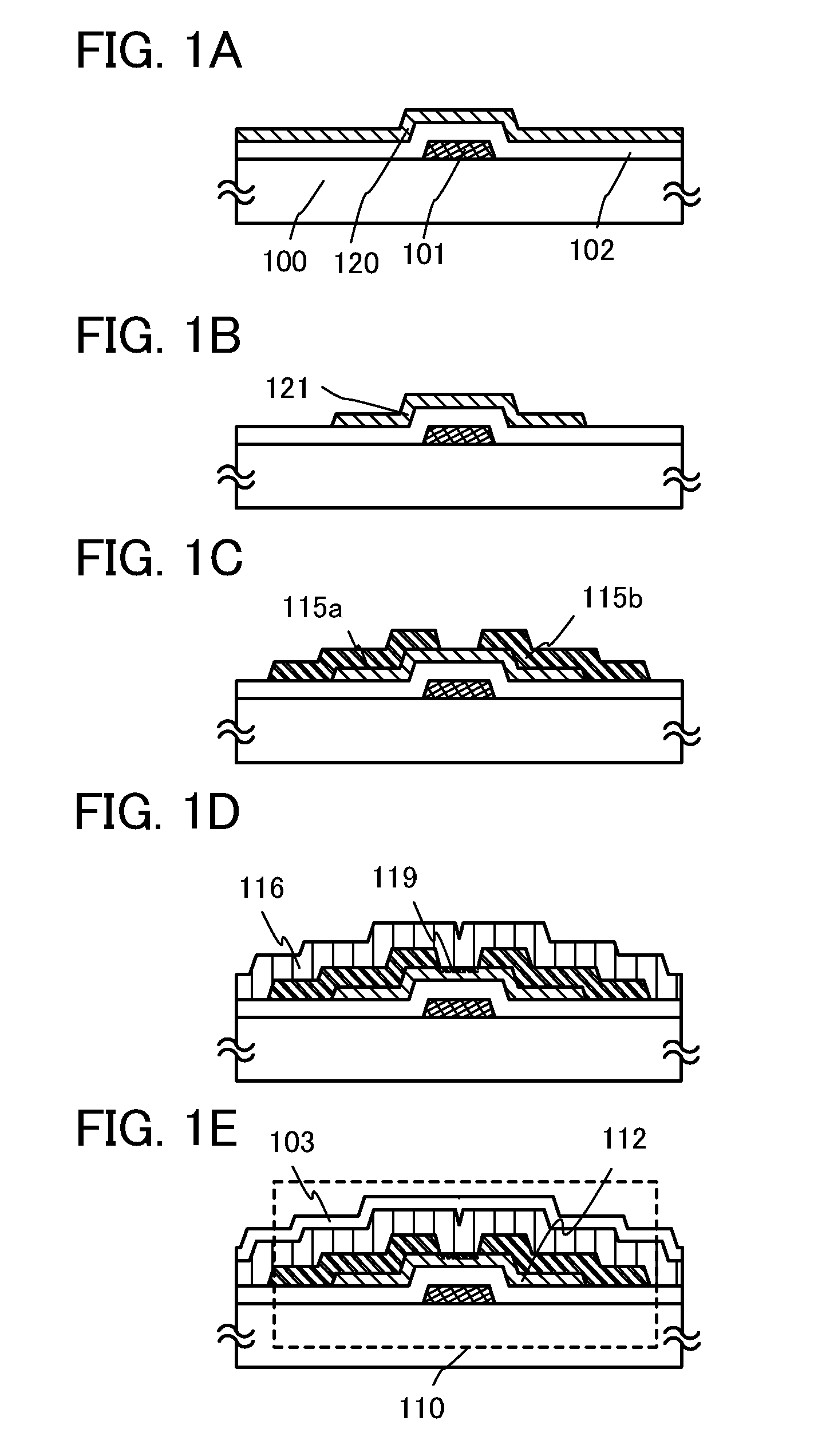
[0055]In this embodiment, an embodiment of a semiconductor device and a manufacturing method of the semiconductor device will be described with reference to FIGS. 1A to 1E. The semiconductor device described in this embodiment is a thin film transistor.

[0056]FIGS. 1A to 1E illustrate an example of a cross-sectional structure of a semiconductor device. A thin film transistor 110 illustrated in FIGS. 1A to 1E has a bottom-gate structure called a channel-etched structure and is also referred to as an inverted staggered thin film transistor.

[0057]The thin film transistor 110 is described using a single-gate thin film transistor; however, a multi-gate thin film transistor including a plurality of channel formation regions can be formed as necessary.

[0058]Hereinafter, a process for manufacturing the thin film transistor 110 over a substrate 100 is described with reference to FIGS. 1A to 1E.

[0059]First, a conductive film is formed over the substrate 100 having an insulating surface, and th...

embodiment 2

[0175]In this embodiment, another example of a thin film transistor which can be applied to a semiconductor device disclosed in this specification will be described.

[0176]In this embodiment, an embodiment of a semiconductor device and a manufacturing method of the semiconductor device will be described with reference to FIGS. 5A to 5E.

[0177]FIGS. 5A to 5E illustrate an example of a cross-sectional structure of a semiconductor device. A thin film transistor 160 illustrated in FIGS. 5A to 5E has a bottom-gate structure called a channel-protective structure (also referred to as a channel-stop structure) and is also referred to as an inverted staggered thin film transistor.

[0178]Although the thin film transistor 160 is described using a single-gate thin film transistor; a multi-gate thin film transistor including a plurality of channel formation regions can be formed as necessary.

[0179]Hereinafter, a process for manufacturing the thin film transistor 160 over a substrate 150 is describe...

embodiment 3

[0212]In this embodiment, another example of a thin film transistor which can be applied to a semiconductor device disclosed in this specification will be described.

[0213]In this embodiment, an embodiment of a semiconductor device and a manufacturing method of the semiconductor device will be described with reference to FIGS. 6A to 6C.

[0214]Although a thin film transistor 190 is described using a single-gate thin film transistor; a multi-gate thin film transistor including a plurality of channel formation regions can be formed as necessary.

[0215]Hereinafter, a process for manufacturing the thin film transistor 190 over a substrate 140 is described with reference to FIGS. 6A to 6C.

[0216]First, a conductive film is formed over the substrate 140 having an insulating surface, and then, a gate electrode layer 181 is formed through a first photolithography step. In this embodiment, a tungsten film with a thickness of 150 nm is formed using a sputtering method as the gate electrode layer 1...


PUM


Abstract

An object is to provide a semiconductor device with stable electric characteristics in which an oxide semiconductor is used. The impurity concentration in the oxide semiconductor layer is reduced in the following manner: a silicon oxide layer including many defects typified by dangling bonds is formed in contact with the oxide semiconductor layer, and an impurity such as hydrogen or moisture (a hydrogen atom or a compound including a hydrogen atom such as H2O) included in the oxide semiconductor layer is diffused into the silicon oxide layer. Further, a mixed region is provided between the oxide semiconductor layer and the silicon oxide layer. The mixed region includes oxygen, silicon, and at least one kind of metal element that is included in the oxide semiconductor.

Description

TECHNICAL FIELD[0001]The present invention relates to a semiconductor device including an oxide semiconductor and a manufacturing method thereof.[0002]In this specification, a semiconductor device means all types of devices which can function by utilizing semiconductor characteristics, and an electrooptic device, a semiconductor circuit, and an electronic appliance are all semiconductor devices.BACKGROUND ART[0003]In recent years, a technique for forming a thin film transistor (TFT) by using a semiconductor thin film (having a thickness of approximately several nanometers to several hundreds of nanometers) formed over a substrate having an insulating surface has attracted attention. Thin film transistors are applied to a wide range of electronic devices such as integrated circuits (ICs) and electro-optical devices, and, in particular, thin film transistors that are used as switching elements in image display devices are urgently developed. There exists a wide variety of metal oxides...

Claims


Application Information

Patent Timeline
Patent Type & Authority Applications(United States)
IPC IPC(8): H01L29/12H01L21/34H05B44/00
CPCH01L21/02554H01L21/02565H01L29/7869H01L27/1225H01L21/02631H01L29/78606H01L21/02164H01L21/02422H01L21/02266H10K59/1213G02F1/1368H01L21/02172H01L21/477H01L27/127H01L29/24H01L29/66969H01L29/78696
Inventor YAMAZAKI, SHUNPEIMIYANAGA, AKIHARUTAKAHASHI, MASAHIROKISHIDA, HIDEYUKISAKATA, JUNICHIRO
Owner SEMICON ENERGY LAB CO LTD
Why Eureka
Try Eureka