
Micro light-emitting diode chip

a light-emitting diode and chip technology, applied in the field of chips, can solve the problems of increasing the cost of the p-type gaas substrate, difficult to control the yield increasing the cost of the n-type gaas substrate, so as to improve the yield in the manufacturing process

Active Publication Date: 2021-11-25
PLAYNITRIDE DISPLAY CO LTD
View PDF0 Cites 1 Cited by
  • Summary
  • Abstract
  • Description
  • Claims
  • Application Information

AI Technical Summary

Benefits of technology

The patent describes a micro-LED chip that can increase the production of successful chips during manufacturing.

Problems solved by technology

The material costs of the N-type GaAs substrate are relatively low, while it is more difficult to control the yield of the N-type GaAs substrate.
However, the cost of the P-type GaAs substrate is at least twice the cost of the N-type GaAs substrate.

Method used


Image

  • Micro light-emitting diode chip
  • Micro light-emitting diode chip
  • Micro light-emitting diode chip

Examples


Embodiment Construction

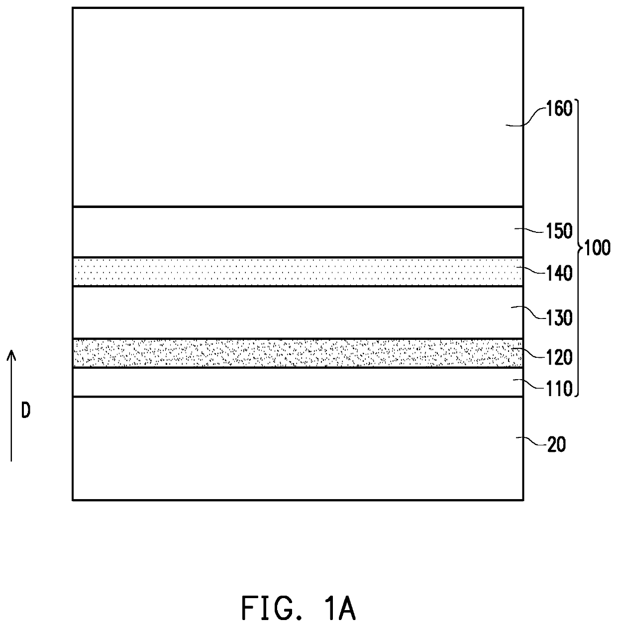
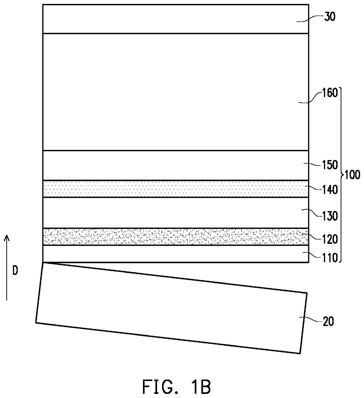
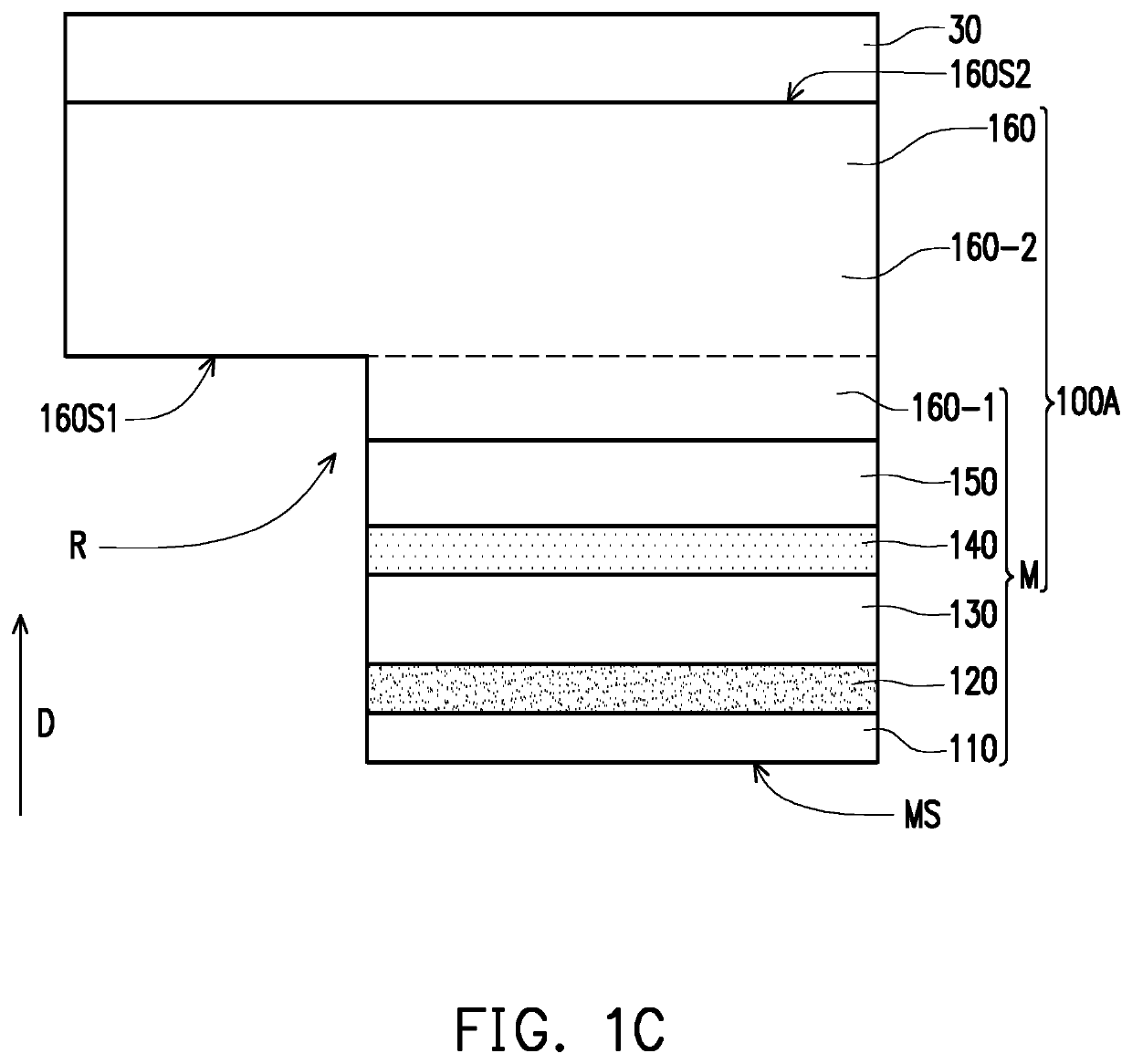
[0024]FIG. 1A to 1E are schematic cross-sectional views of a manufacturing process of a micro-LED chip according to an embodiment of the disclosure. With reference to FIG. 1A to FIG. 1E, an embodiment of the disclosure provides a micro-LED chip 10A, which includes a GaAs epitaxial structure layer 100A, a first electrode 200, and a second electrode 300. In the embodiment, the micro-LED chip 10A is, for instance, a red light or an infrared light micro-LED chip, while the disclosure is not limited thereto.

[0025]As shown in FIG. 1A, a GaAs epitaxial structure layer 100 is formed on a first substrate 20. In the embodiment, a material of the first substrate 20 is lightly-doped N-GaAs or neutral GaAs. The GaAs epitaxial structure layer 100 includes an N-type contact layer 110, a tunneling junction layer 120, a P-type semiconductor layer 130, a light-emitting layer 140, an N-type semiconductor layer 150, and an N-type window layer 160 sequentially along a stacking direction D. That is, the ...


PUM

PropertyMeasurementUnit
thicknessaaaaaaaaaa
thicknessaaaaaaaaaa
temperatureaaaaaaaaaa

Abstract

A micro light-emitting diode (micro-LED) chip adapted to emit a red light or an infrared light is provided. The micro-LED chip includes a GaAs epitaxial structure layer, a first electrode, and a second electrode. The GaAs epitaxial structure layer includes an N-type contact layer, a tunneling junction layer, a P-type semiconductor layer, a light-emitting layer, an N-type semiconductor layer, and an N-type window layer along a stacking direction. The first electrode electrically contacts the N-type contact layer. The second electrode electrically contacts the N-type window layer.

Description

CROSS-REFERENCE TO RELATED APPLICATION[0001]This application claims the priority benefit of Taiwan patent application serial no. 109116474, filed on May 19, 2020. The entirety of the above-mentioned patent application is hereby incorporated by reference herein and made a part of specification.BACKGROUNDTechnical Field[0002]The disclosure relates to a chip, and in particular to a micro light-emitting diode (micro-LED) chip.Description of Related Art[0003]In general, a red light is generated by adopting an N-type gallium arsenide (GaAs) substrate as an epitaxial growth substrate, and after an N-type semiconductor layer is formed on the growth substrate, a light-emitting layer and a P-type semiconductor layer are sequentially formed. The material costs of the N-type GaAs substrate are relatively low, while it is more difficult to control the yield of the N-type GaAs substrate.[0004]Although a P-type GaAs substrate may also be adopted as the epitaxial growth substrate, and after the P-t...

Claims


Application Information

Patent Timeline
Patent Type & Authority Applications(United States)
IPC IPC(8): H01L33/30H01L33/00H01L33/62
CPCH01L33/305H01L33/62H01L33/0008H01L33/04H01L33/382
Inventor WANG, TZU-WENFANG, HSIN-CHIAO
Owner PLAYNITRIDE DISPLAY CO LTD
Learn More