Substrate integrated waveguide fed antenna
a waveguide and integrated technology, applied in the direction of linear waveguide fed arrays, individual energised antenna arrays, particular array feeding systems, etc., can solve the problems of inconvenient application in compact devices, and antenna elements that are not suitable for compact devices
- Summary
- Abstract
- Description
- Claims
- Application Information
AI Technical Summary
Benefits of technology
Problems solved by technology
Method used
Image
Examples
Embodiment Construction
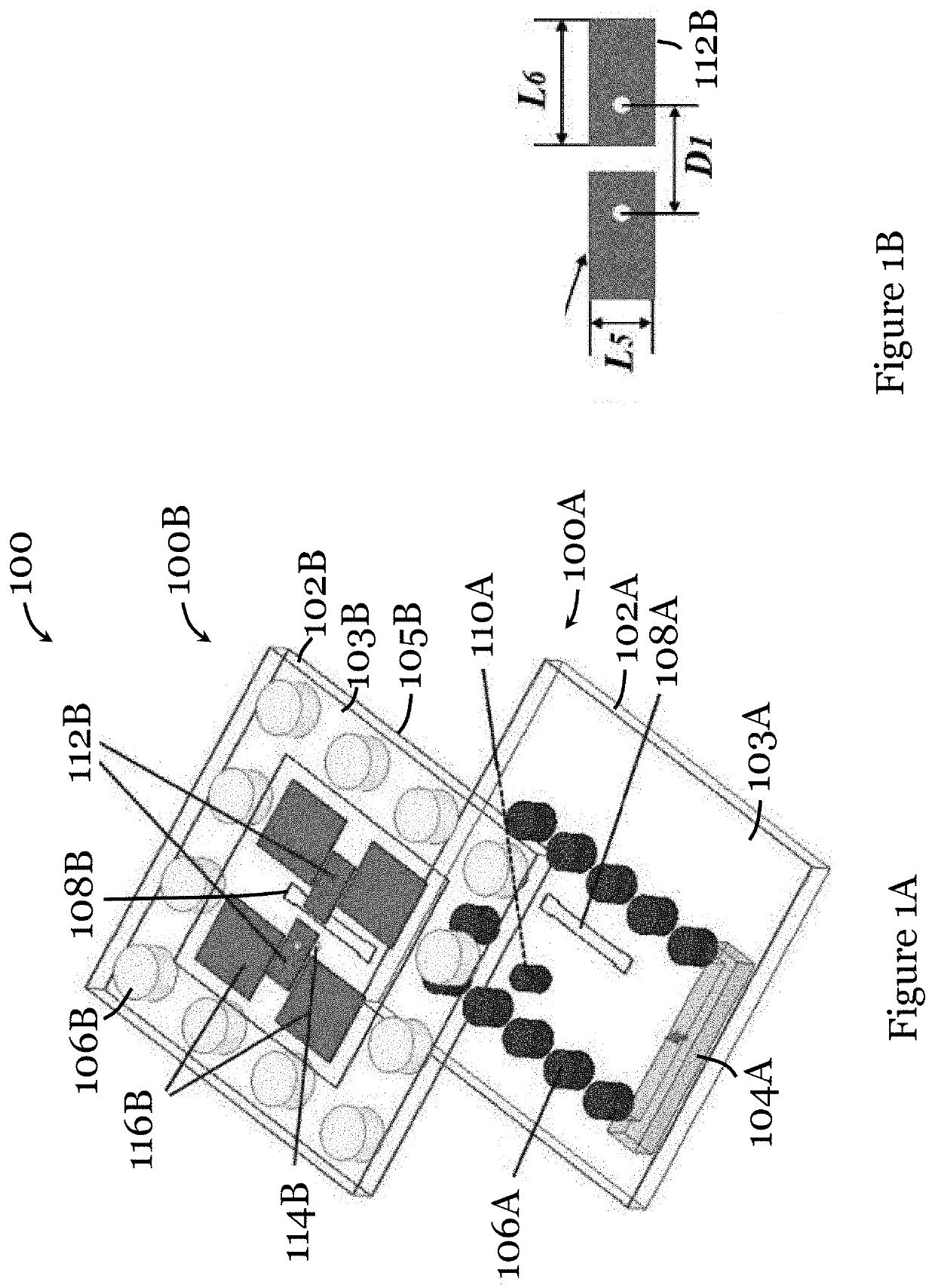
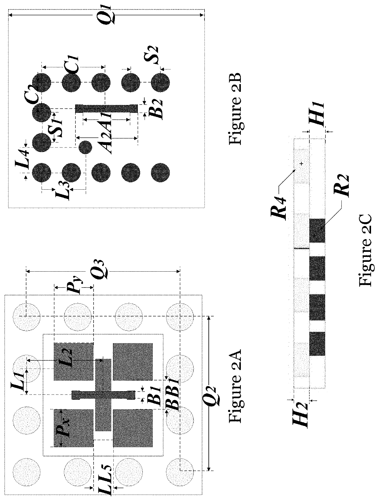
[0096]FIGS. 1A to 2C shows a substrate integrated waveguide fed antenna 100 in one embodiment of the invention. The antenna 100 includes two substrates, an upper substrate 100B and a lower substrate 100A. The lower substrate 100A is essentially a substrate integrated waveguide, which provides a feed structure. The lower substrate 100A includes a substrate layer 102A with an upper conductive surface 103A formed by copper. A feed port 104A and multiple vias 106A are arranged in, e.g., extend through, the substrate layer 102A. The vias 106A are arranged in a generally U-shaped array in plan view. The upper conductive surface 103A is a slotted conductive surface having a dumbbell shaped slot 108A. This dumbbell shaped slot 108A is arranged to be aligned and operably coupled with another dumbbell shaped slot 108B formed on the lower conductive surface of the upper substrate 100B. In this example, the two dumbbell shaped slots 108A, 108B have similar form (an elongated central slot portio...
PUM
 Abstract
Description
Claims
Application Information


