
Semiconductor structure

a technology of semiconductor devices and structures, applied in the direction of semiconductor devices, electrical equipment, nanotechnology, etc., can solve the problems of adverse effects on the electrical properties of semiconductor devices

Active Publication Date: 2021-12-30
SEMICON MFG INT (SHANGHAI) CORP +1
View PDF1 Cites 2 Cited by
  • Summary
  • Abstract
  • Description
  • Claims
  • Application Information

AI Technical Summary

Benefits of technology

This approach improves the performance of both peripheral and core devices by reducing self-heating in peripheral devices and body effects in core devices, enhancing overall semiconductor device performance and reducing leakage current.

Problems solved by technology

Accordingly, the leakage current is generated; and, ultimately, the electrical properties of the semiconductor devices are adversely affected.

Method used


Image

  • Semiconductor structure
  • Semiconductor structure
  • Semiconductor structure

Examples


Embodiment Construction

[0012]Reference will now be made in detail to exemplary embodiments of the disclosure, which are illustrated in the accompanying drawings. Wherever possible, the same reference numbers will be used throughout the drawings to refer to the same or like parts.

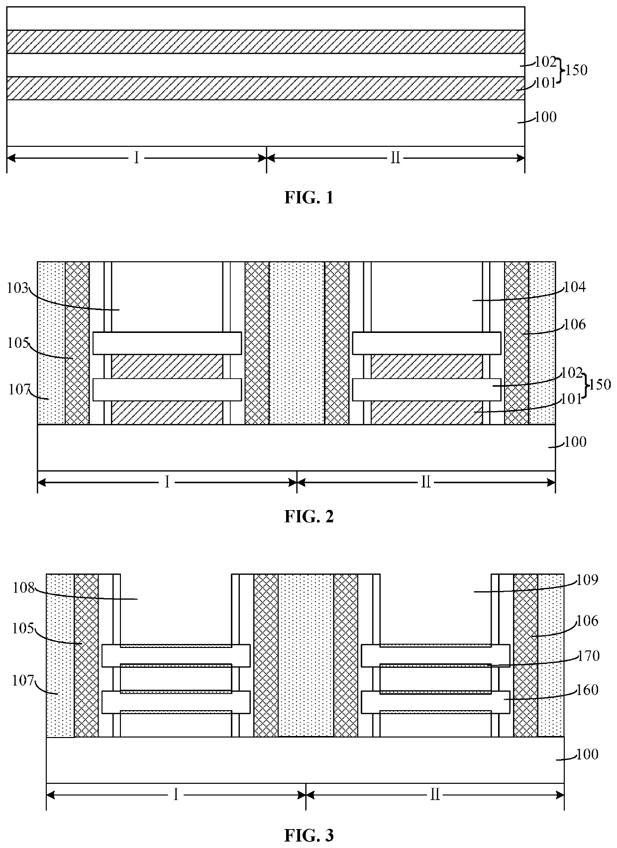
[0013]FIGS. 1-3 illustrate structures corresponding to certain stages during a fabrication process of a semiconductor structure

[0014]As shown in FIG. 1, the fabrication process includes providing a semiconductor substrate 100. The semiconductor substrate 100 includes a first region I and a second region II. A fin material layer extending from the first region Ito the second region II is formed on the surface of the semiconductor substrate 100. The fin material layer includes a plurality of multiple-layer stacked fin units 150. Each fin unit includes a sacrificial layer 101 and a nanowire material layer 102 on the sacrificial layer 101. A mask layer (not shown) is formed on the fin material layer. The mask layer exposes portions of...


PUM


Abstract

A semiconductor structure is provided. The semiconductor structure includes a semiconductor substrate having a first region and a second region; first nanowires formed over the first region of the semiconductor substrate; second nanowires with a diameter smaller than a diameter of the first nanowires formed over the second region of the semiconductor substrate; a first gate layer formed around the first nanowires; and a second gate layer formed around the second nanowires.

Description

CROSS-REFERENCES TO RELATED APPLICATIONS[0001]This application is a divisional application of U.S. patent application Ser. No. 16 / 419,830, filed on May 22, 2019, which claims the priority of Chinese patent application No. 201810567937.5, filed on Jun. 5, 2018, the entirety of which is incorporated herein by reference.FIELD OF THE DISCLOSURE[0002]The present disclosure generally relates to the field of semiconductor manufacturing and, more particularly, relates to semiconductor structures and fabrication methods.BACKGROUND[0003]With the continuous increase of the device density and integration level of semiconductor devices, the size of the gate of transistor has become smaller and smaller. The reduction of the size of the gate of the transistor causes the transistor to have a short channel effect. Accordingly, the leakage current is generated; and, ultimately, the electrical properties of the semiconductor devices are adversely affected.[0004]To overcome the short channel effect and...

Claims


Application Information

Patent Timeline
Patent Type & Authority Applications(United States)
IPC IPC(8): H01L29/06H01L29/423H01L29/78H01L21/02H01L21/308H01L29/66H01L21/8234H01L29/10H01L29/08H01L27/088
CPCH01L29/0673H01L29/6659H01L29/7843H01L21/0217H01L21/02532H01L21/308H01L21/02236H01L29/66545H01L21/823418H01L29/6656H01L29/1033H01L21/823431H01L29/0847H01L27/0886H01L21/823412H01L29/42392H01L27/088H01L29/775B82Y10/00H01L29/78696H01L29/513H01L29/7845H01L29/66439H01L29/0653H01L29/401
Inventor ZHANG, HUAN YUNWU, JIAN
Owner SEMICON MFG INT (SHANGHAI) CORP
Learn More