Check patentability & draft patents in minutes with Patsnap Eureka AI!

Resistive memory device

Active Publication Date: 2022-01-13
SAMSUNG ELECTRONICS CO LTD
View PDF2 Cites 2 Cited by
  • Summary
  • Abstract
  • Description
  • Claims
  • Application Information

AI Technical Summary

Benefits of technology

The patent text describes a new design for a memory device that improves its performance and reduces manufacturing costs. The design also provides enough margin for both reading and writing operations.

Problems solved by technology

However, the large number of drivers causes the resistive memory device to occupy a large area, thereby increasing manufacturing costs.

Method used


Image

  • Resistive memory device
  • Resistive memory device
  • Resistive memory device

Examples


Embodiment Construction

[0031]Hereinafter, one or more embodiments of the inventive concept will be described in detail with reference to the attached drawings. Like reference symbols in the drawings denote like elements, and repeated descriptions thereof are omitted.

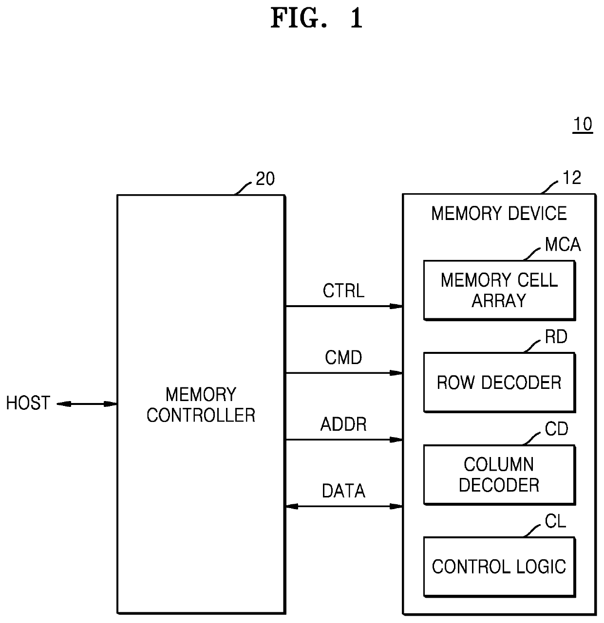
[0032]FIG. 1 is a block diagram of a memory system including a resistive memory device, according to embodiments.

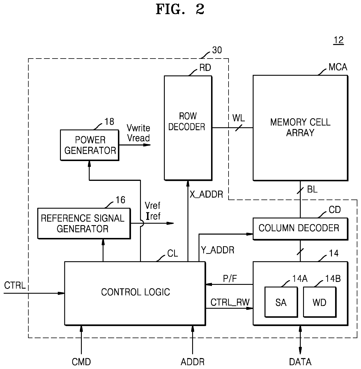
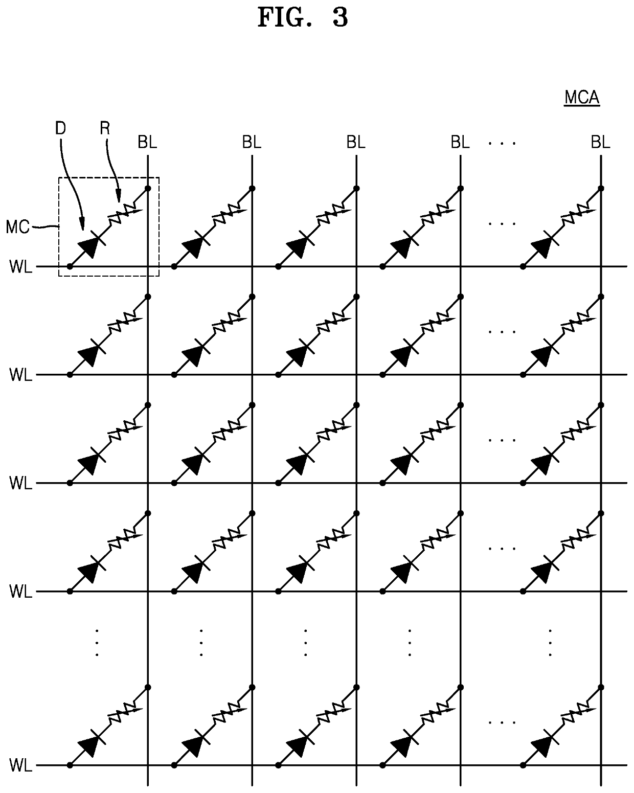
[0033]Referring to FIG. 1, a memory system 10 includes a memory device 12 and a memory controller 20 (e.g., a control circuit). The memory device 12 includes a memory cell array MCA, a row decoder RD (e.g., a decoder circuit), a column decoder CD (e.g., a decoder circuit), and control logic CL (e.g., a logic circuit).

[0034]The memory controller 20 may control the memory device 12 to read data stored in the memory device 12 or write data to the memory device 12, in response to a write / read request from a host. The memory controller 20 may control performance of a program (or write) operation, a read operation, and an erase operation ...


PUM


Abstract

A resistive memory device includes a first word line extending in a first horizontal direction, a second word line extending on the first word line in the first horizontal direction, a third word line extending on the second word line in the first horizontal direction, a first bit line extending between the first and second word lines in a second horizontal direction, a second bit line extending between the second and third word lines in the second horizontal direction, and memory cells respectively arranged between the first word line and the first bit line, between the first bit line and the second word line, between the second word line and the second bit line, and between the second bit line and the third word line. A thickness of the second word line is greater than a thickness of each of the first word line and the third word line.

Description

CROSS-REFERENCE TO RELATED APPLICATIONS[0001]This non-provisional U.S. patent application claims priority under 35 U.S.C. § 119 to Korean Patent Application No. 10-2020-0084356, filed on Jul. 8, 2020, and Korean Patent Application No. 10-2020-0174730, filed on Dec. 14, 2020, in the Korean Intellectual Property Office, the disclosures of which are incorporated by reference in their entireties herein.1. TECHNICAL FIELD[0002]The inventive concept relates to a memory device, and more particularly, to a resistive memory device having a cross-point array structure.2. DISCUSSION OF RELATED ART[0003]A resistive memory device includes several memory cells, where a value of a resistance of each memory cell represents a certain data state of the corresponding memory cell. Examples of a resistive memory device include a resistive random-access memory and phase-change memory.[0004]In a resistive memory device having a three-dimensional cross-point stack structure, a memory cell is arranged at an...

Claims


Application Information

Patent Timeline
IPC IPC(8): G11C13/00H01L27/24H01L45/00
CPCG11C13/0028G11C13/0026H01L27/2427H01L45/122H01L45/1675G11C13/0004H01L27/2463G11C2213/72H01L45/141H01L45/06G11C2213/71H10B63/24H10B63/30H10B63/84H10N70/231H10N70/826H10N70/8822H10N70/8825H10N70/8828H10B63/80H10N70/821H10N70/063H10N70/882
Inventor TERAI, MASAYUKI
Owner SAMSUNG ELECTRONICS CO LTD
Features
  • R&D
  • Intellectual Property
  • Life Sciences
  • Materials
  • Tech Scout
  • Unparalleled Data Quality
  • Higher Quality Content
  • 60% Fewer Hallucinations
Learn More