Semiconductor memory device and method of fabricating the same

Pending Publication Date: 2022-03-10
SAMSUNG ELECTRONICS CO LTD
View PDF0 Cites 0 Cited by
  • Summary
  • Abstract
  • Description
  • Claims
  • Application Information

AI Technical Summary

Benefits of technology

The patent describes a semiconductor memory device that has better electrical properties.

Problems solved by technology

To meet this demand, complexity and / or integration density of semiconductor devices are being increased.

Method used


Image

  • Semiconductor memory device and method of fabricating the same
  • Semiconductor memory device and method of fabricating the same
  • Semiconductor memory device and method of fabricating the same

Examples


Embodiment Construction

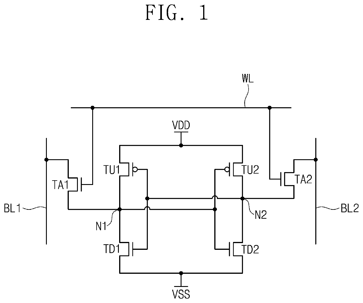
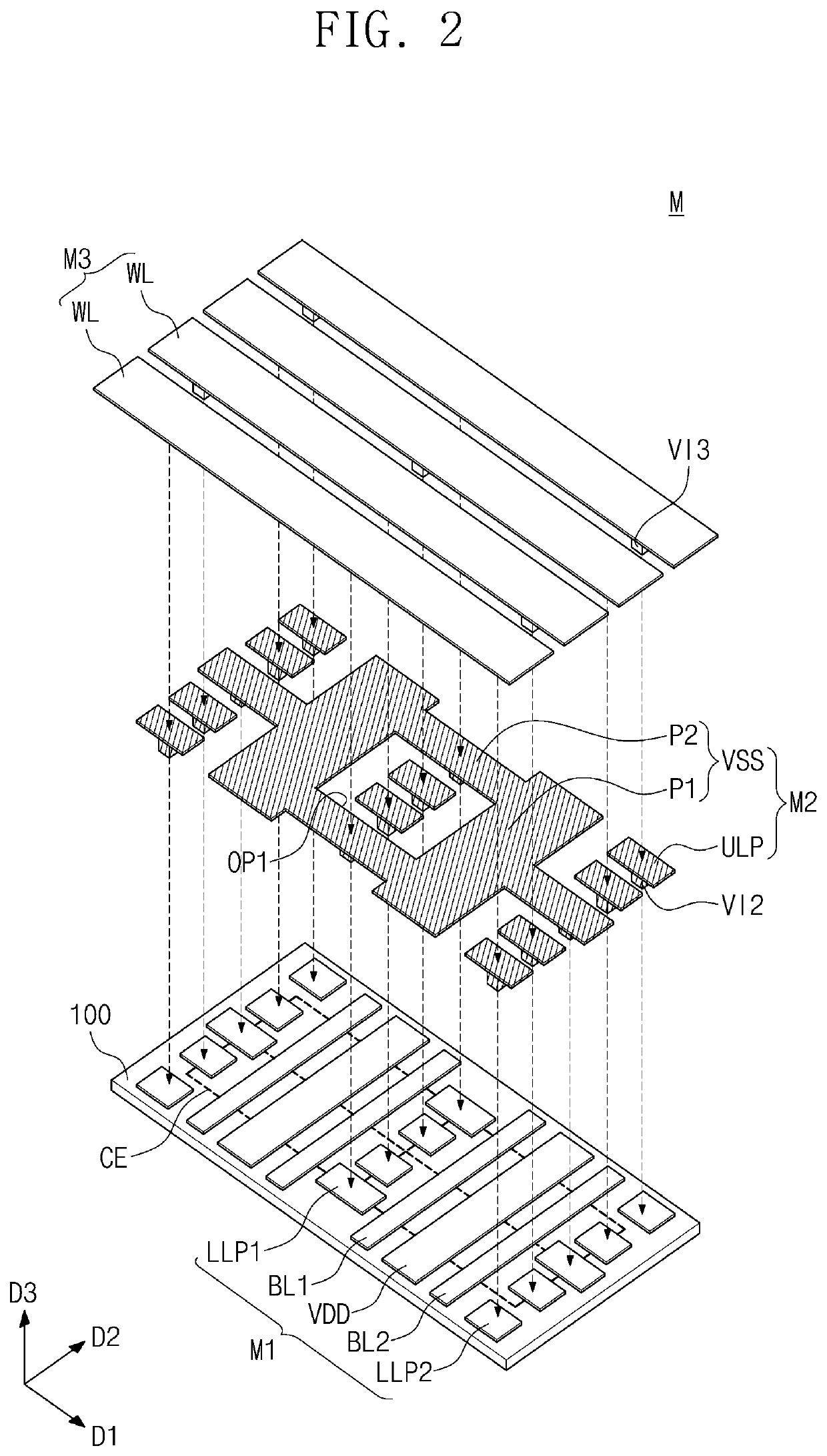
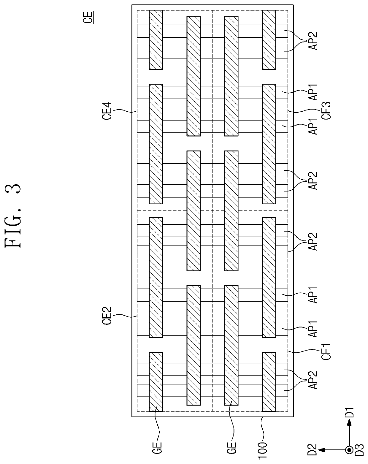
[0025]FIG. 1 is an equivalent circuit diagram illustrating a static random access memory (SRAM) cell according to an embodiment of the disclosure.

[0026]Referring to FIG. 1, the SRAM cell may include a first pull-up transistor TU1, a first pull-down transistor TD1, a second pull-up transistor TU2, a second pull-down transistor TD2, a first pass-gate transistor TA1, and a second pass-gate transistor TA2. The first and second pull-up transistors TU1 and TU2 may be P-channel metal-oxide semiconductor (PMOS) transistors. The first and second pull-down transistors TD1 and TD2 and the first and second pass-gate transistors TA1 and TA2 may be N-channel metal-oxide semiconductor (NMOS) transistors.

[0027]A first source / drain of the first pull-up transistor TU1 and a first source / drain of the first pull-down transistor TD1 may be connected to a first node N1. A second source / drain of the first pull-up transistor TU1 may be connected to a power line VDD, and a second source / drain of the first p...


PUM


Abstract

A semiconductor memory device includes a static random access memory (SRAM) cell that is provided on a substrate and includes a pass-gate transistor, a pull-down transistor, and a pull-up transistor. Each of the pass-gate transistor, the pull-down transistor, and the pull-up transistor includes an active fin protruding above a device isolation layer, a gate electrode on the active fin, and a gate insulating layer between the active fin and the gate electrode. The gate insulating layer of the pull-down transistor includes a first dipole element. The highest concentration of the first dipole element of the gate insulating layer of the pull-down transistor is higher than the highest concentration of the first dipole element of the gate insulating layer of the pass-gate transistor.

Description

CROSS-REFERENCE TO RELATED APPLICATIONS[0001]This U.S. non-provisional patent application claims priority under 35 U.S.C. § 119 to Korean Patent Application No. 10-2020-0115272, filed on Sep. 9, 2020, in the Korean Intellectual Property Office, the entire contents of which are hereby incorporated by reference.BACKGROUND OF THE RELATED ART[0002]The present disclosure relates to a semiconductor memory device and a method of fabricating, and in particular, to a semiconductor memory device including a static random access memory (SRAM) cell and a method of fabricating the same.[0003]Due to their small-sized, multifunctional, and / or low-cost characteristics, semiconductor devices are being esteemed as important elements in the electronics industry. The semiconductor devices are classified into a semiconductor memory device for storing data, a semiconductor logic device for processing data, and a hybrid semiconductor device including both of memory and logic elements. As the electronic in...

Claims


Application Information

Patent Timeline
IPC IPC(8): H01L27/11H01L27/092H01L29/78H01L29/08H01L29/45H01L29/51H01L29/06H01L29/423H01L29/49H01L29/786H01L21/02H01L21/285H01L21/8238H01L29/66
CPCH01L27/1108H01L29/66742H01L29/7851H01L29/0847H01L29/45H01L29/516H01L29/78391H01L29/0665H01L29/42392H01L29/4908H01L29/78618H01L29/78696H01L21/0259H01L21/28518H01L21/823807H01L21/823814H01L21/823821H01L21/823857H01L21/823871H01L29/66545H01L29/66795H01L29/6684H01L27/0924H01L29/775H01L27/092H01L27/0207H01L29/7848H01L29/165H01L29/513H01L29/41766H01L29/4966H01L21/76895H01L29/0673B82Y10/00H10B10/125H01L29/785H01L29/51H10B10/12
Inventor HONG, HEE BUMSHIN, HEESUNGLEE, HOJOONJUNG, YOUNGHUNHONG, CHANG-MIN
Owner SAMSUNG ELECTRONICS CO LTD
Why Eureka
Try Eureka