Fabricating method of polycrystalline silicon thin film transistor

Active Publication Date: 2003-07-03
LG DISPLAY CO LTD
View PDF4 Cites 5 Cited by
  • Summary
  • Abstract
  • Description
  • Claims
  • Application Information

AI Technical Summary

Benefits of technology

[0015] An object of the present invention is to provide a fabricating method for a polycrystalline silicon transistor having improved electric characteristics.
[0016] Another object of the present invention is to provide a fabricating method of a thin film transistor having an improved reliability by forming an active layer having an improved step coverage property.
[0017] Another object of the present invention is to provide a chemical to eliminate a metal silicide residue that remains on a surface after patterning an active layer.

Problems solved by technology

However, since the hydrogenated amorphous silicon has a disordered atomic arrangement in that weak silicon-silicon (Si--Si) bonds and dangling bonds exist in the hydrogenated amorphous silicon.
As a result, this metastability makes the TFT unstable.
Electrical characteristics of the hydrogenated amorphous silicon are especially degraded due to light irradiation.
Further, a TFT using the hydrogenated amorphous silicon is hard to use in a driving circuit due to degraded electric characteristics such as a low field effect mobility between about 0.1 cm.sup.2 / Vsec to about 1.0 cm.sup.2 / Vsec, and poor reliability.
The driving IC and its packaging increase the production cost of an LCD device.
Thus, bonding of the TCP and the substrate including the a-Si TFT becomes harder.
In the high temperature crystallization process, a high cost quartz substrate is required to be used because the process temperature is around 1000.degree. C. that is above a strain temperature of a glass substrate.
Moreover, since a polycrystalline silicon thin film fabricated through the high temperature crystallization process has a high surface roughness and a poor crystallinity (e.g., fine grain), a high temperature p-Si TFT has worse electrical characteristics than a low temperature p-Si TFT.
The poor step coverage causes process inferiority, such as a lower pattern resolution.

Method used


Image

  • Fabricating method of polycrystalline silicon thin film transistor
  • Fabricating method of polycrystalline silicon thin film transistor
  • Fabricating method of polycrystalline silicon thin film transistor

Examples


Embodiment Construction

[0026] Reference will now be made in detail to the preferred embodiments of the present invention, examples of which are illustrated in the accompanying drawings.

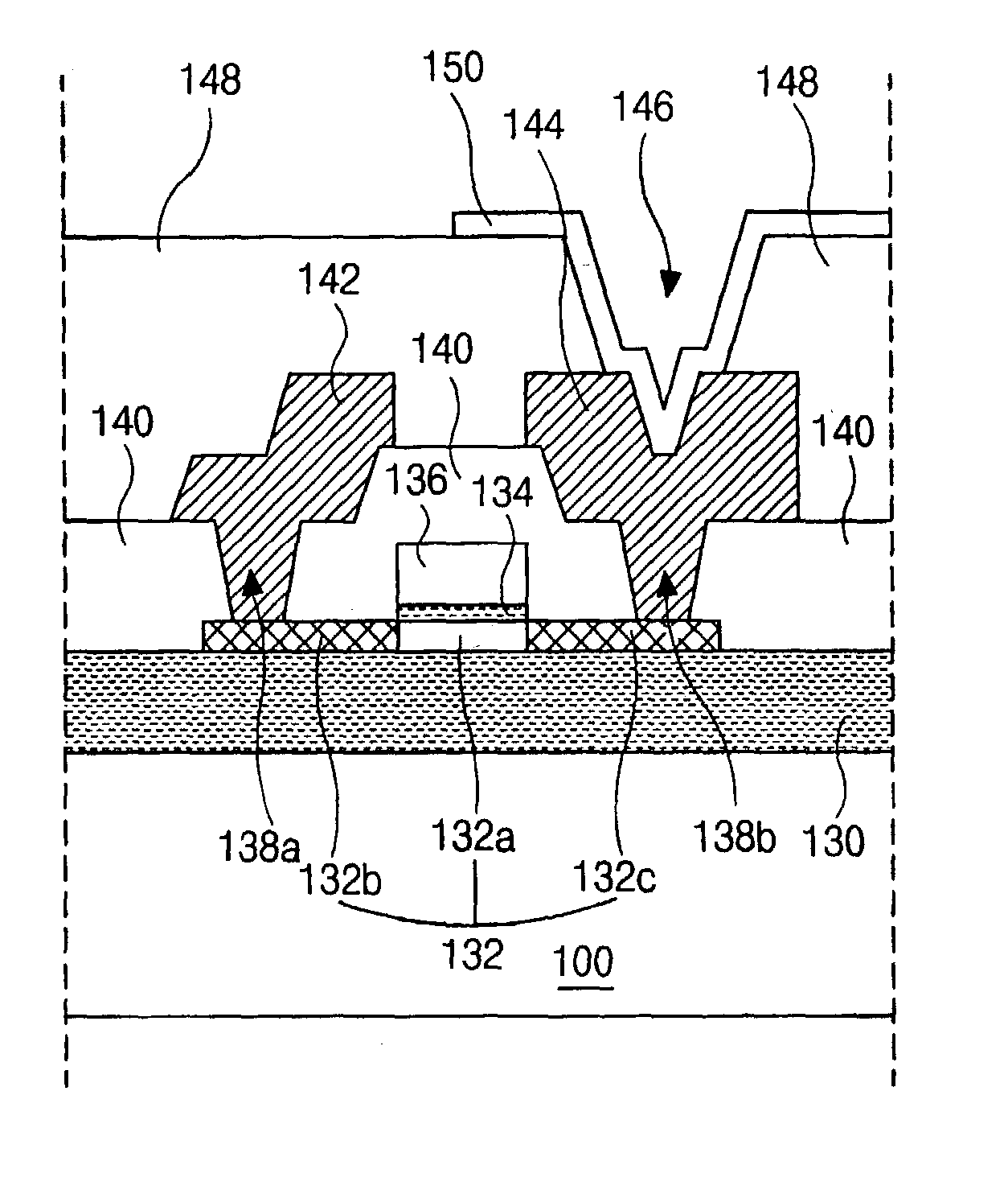
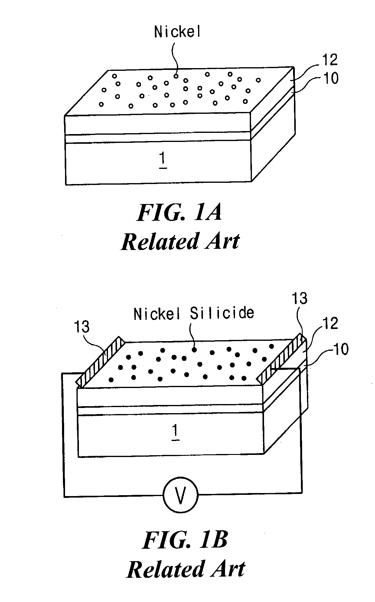
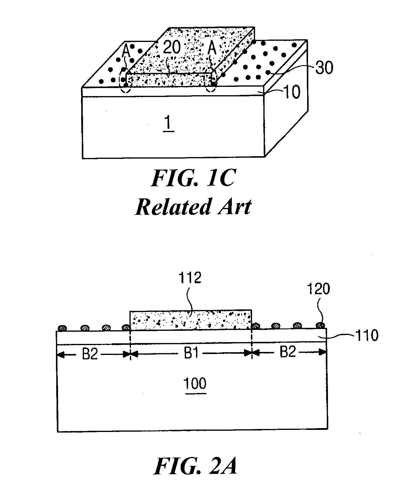
[0027] In this example, hydrofluoric acid (HF) and hydrogen peroxide (H.sub.2O.sub.2) are used for cleaning. After a polycrystalline silicon layer crystallized through a low temperature crystallization method using nickel silicide as a crystallization catalyst is patterned to form an active layer, a nickel silicide residue remains on a buffer layer of silicon oxide (SiO.sub.x). A solution including hydrofluoric acid (HF) and hydrogen peroxide (H.sub.2O.sub.2) may be used to eliminate the nickel silicide residue. Here, it is important to adjust concentrations of control hydrofluoric acid (HF) and hydrogen peroxide (H.sub.2O.sub.2) such that the solution does not cause damages to the active layer.

[0028] FIGS. 2A to 2C are schematic cross-sectional views illustrating a part of a fabricating process of a polycrystalline silicon...


PUM


Abstract

A fabricating method of a polycrystalline silicon thin film transistor includes forming a polycrystalline silicon layer on a substrate having first and second regions through a crystallization process using nickel silicide (NiSi.sub.x) as a catalyst, patterning the polycrystalline silicon layer to form an active layer at the first region, leaving a nickel silicide residue at the second region, etching the nickel silicide residue with a solution including hydrofluoric acid (HF) and hydrogen peroxide (H.sub.2O.sub.2), forming a gate electrode over the active layer and forming a source and drain in the active layer.

Description

[0001] The present invention claims the benefit of the Korean Patent Application No. 2001-86427 filed in Korea on Dec. 27, 2001, which is hereby incorporated by reference in its entirety.BACKGROUND OF THE INVENTION[0002] 1. Field of the Invention[0003] The present invention relates to a liquid crystal display device, and more particularly, to a fabricating method of a poly crystalline thin film transistor that is used as a switching element of a liquid crystal display device.[0004] 2. Discussion of the Related Art[0005] In the field of flat panel display (FPD), active matrix liquid crystal display (AMLCD) devices are widely used. In the LCD devices, a thin film transistor (TFT) is used as a switching element that manipulates the light transmittance of a pixel region by adjusting a voltage applied to a liquid crystal layer of the pixel region. These LCD devices are referred to as thin film transistor liquid crystal display (TFT-LCD) devices. Hydrogenated amorphous silicon (a-Si:H) is...

Claims


Application Information

Patent Timeline
IPC IPC(8): C09K13/04H01L21/00H01L21/20H01L21/302H01L21/3213H01L21/336H01L21/461H01L29/786
CPCH01L21/2022H01L21/32134H01L29/78675H01L29/66757H01L21/32139H01L21/02532H01L21/02672H01L29/786
Inventor SEO, HYUN-SIKKIM, BINN
Owner LG DISPLAY CO LTD
Why Eureka
Try Eureka