

Semiconductor package and method of fabricating the same
- Summary
- Abstract
- Description
- Claims
- Application Information
AI Technical Summary
Benefits of technology
Problems solved by technology
Method used
Image

Examples
Embodiment Construction
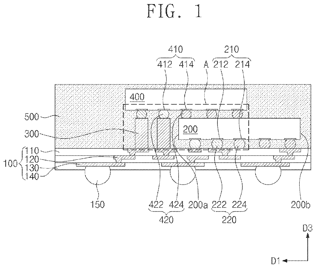
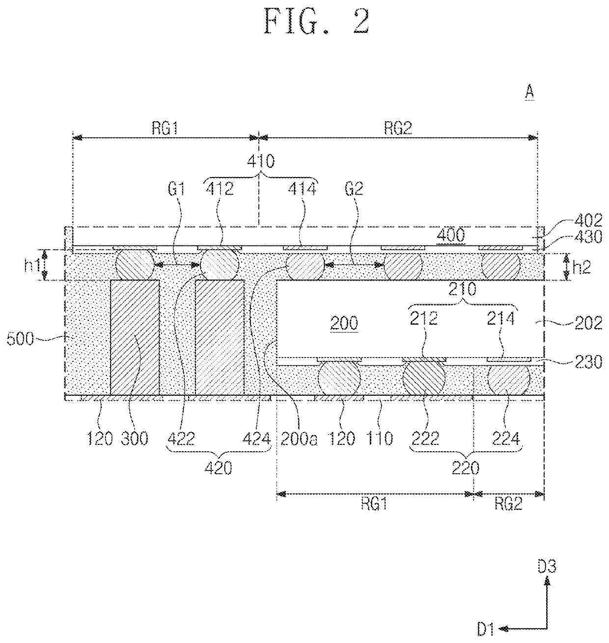
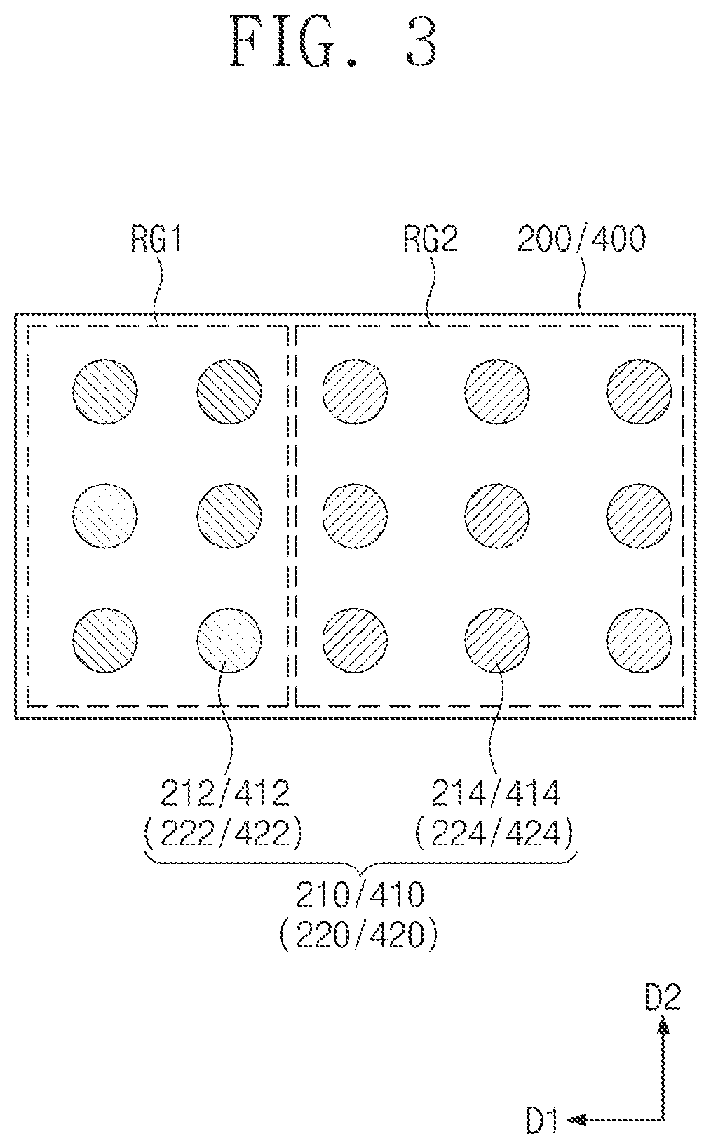
[0023]FIG. 1 illustrates a sectional view of a semiconductor package according to embodiments of the inventive concepts. FIG. 2 illustrates an enlarged sectional view of portion ‘A’ of FIG. 1. FIG. 3 illustrates a plan view of arrangements of soldering structures in first and second semiconductor chips of a semiconductor package according to embodiments of the inventive concepts. FIGS. 4 to 6 illustrate enlarged sectional views of the portion ‘A’ of FIG. 1.
[0024]Referring to FIGS. 1 and 2, a substrate may be provided. The substrate 100 may be a redistribution substrate. For example, the substrate 100 may include at least one substrate interconnection layer. In an embodiment, the substrate 100 may include a plurality of substrate interconnection layers, which are sequentially stacked, and in this case, each of the substrate interconnection layers may include a substrate insulating layer 110 and a substrate interconnection pattern 120 in the substrate insulating layer 110. The substra...
PUM
 Abstract
Description
Claims
Application Information