Semiconductor device

a technology of semiconductors and devices, applied in semiconductor devices, semiconductor/solid-state device details, cooling/ventilation/heating modifications, etc., can solve the problems of uneven cooling effect of modules, insufficient flow rate of coolant, and high pressure loss between fins, so as to ensure rigidity and ensure cooling performan

Pending Publication Date: 2022-03-17
FUJI ELECTRIC CO LTD
View PDF0 Cites 1 Cited by
  • Summary
  • Abstract
  • Description
  • Claims
  • Application Information

AI Technical Summary

Benefits of technology

[0010]According to the present invention, it is possible to ensure cooling performance while also ensuring rigidity.

Problems solved by technology

However, the gaps between the fins tend to have high pressure loss.
As a result, the flow rate of coolant cannot be ensured adequately all the way to the base of the plurality of fins, and an uneven cooling effect of the module may occur.
Also, the cooling fin base on which the plurality of fins are formed may undergo thermal deformation during the manufacturing process.
However, increasing the thickness causes an increase in thermal resistance, and may result in influencing the original thermal conductivity of the cooler.

Method used


Image

  • Semiconductor device
  • Semiconductor device
  • Semiconductor device

Examples


Embodiment Construction

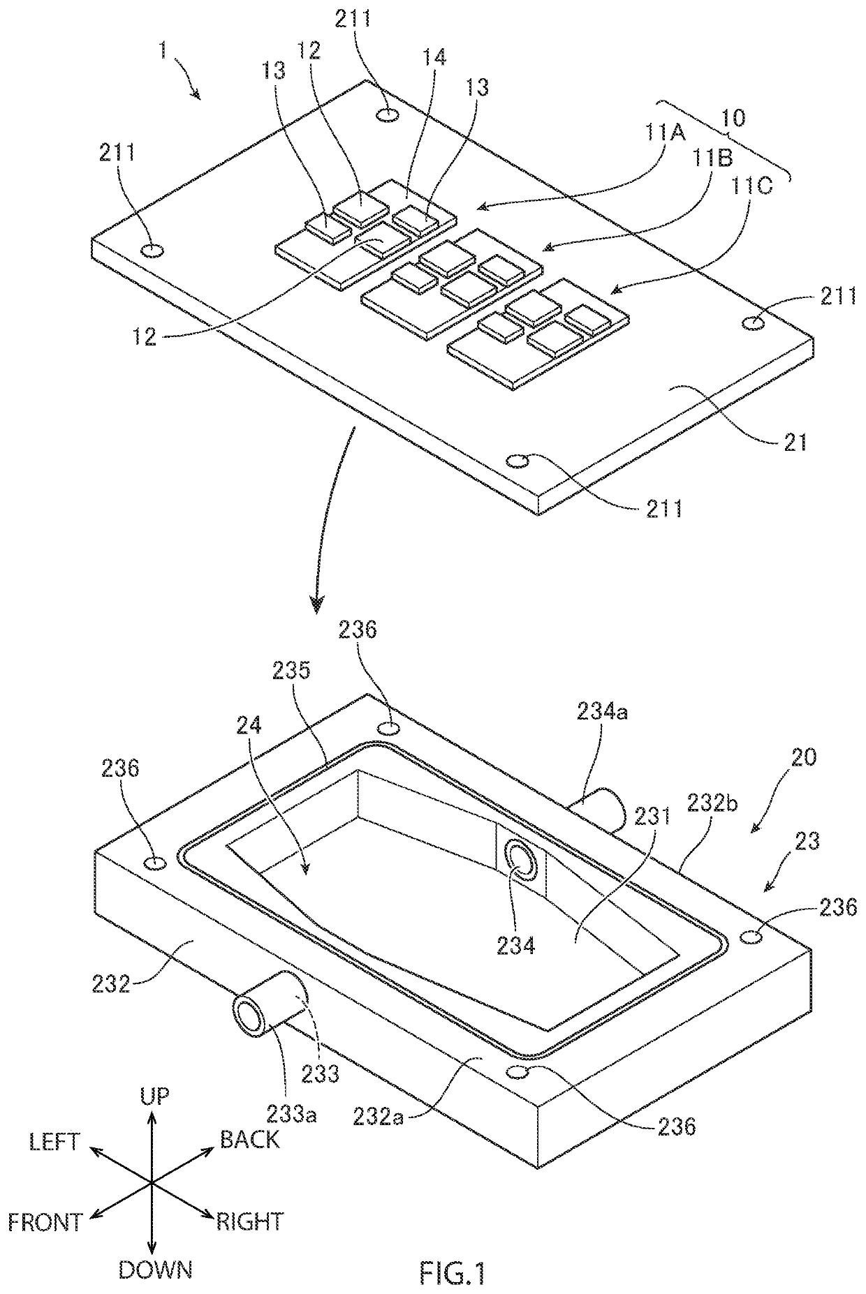
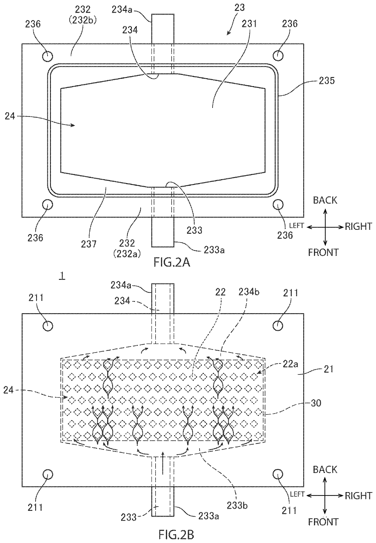
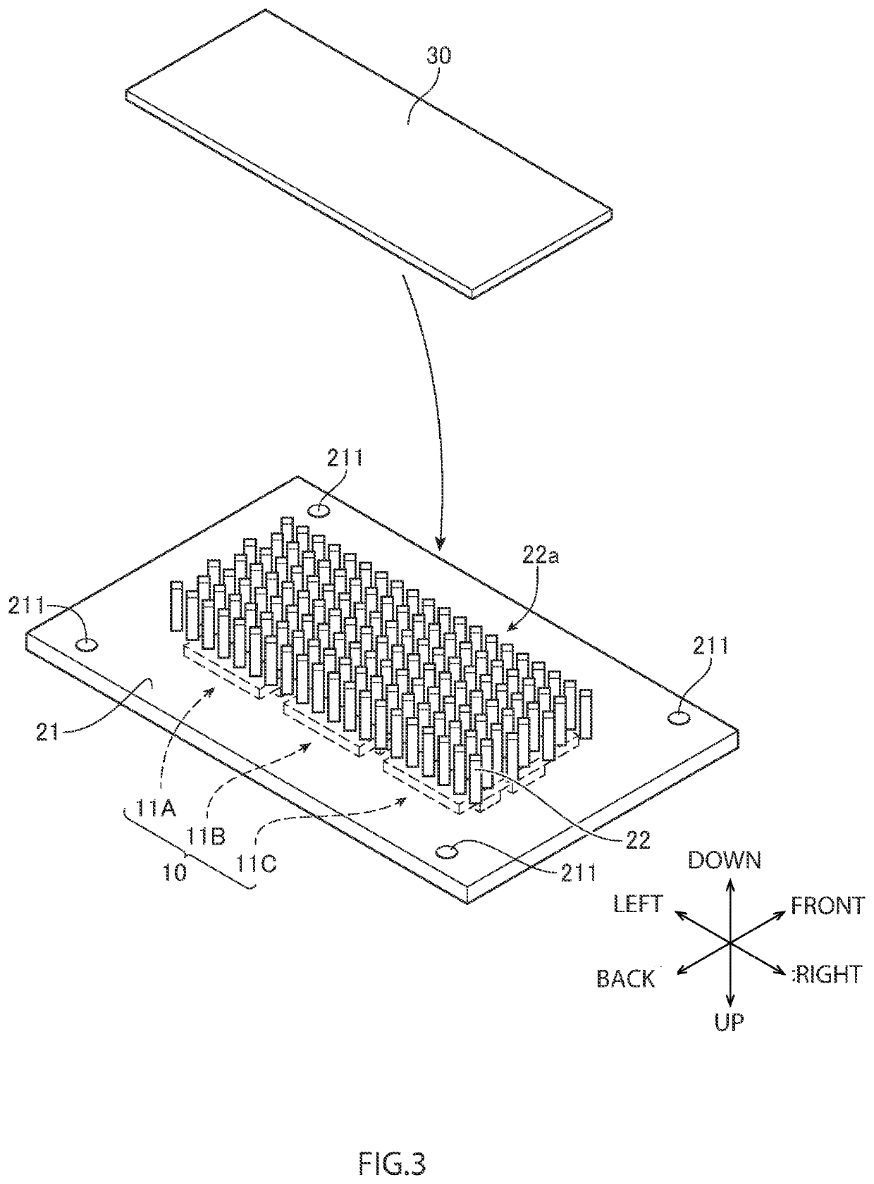
[0021]Hereinafter, the configuration of a semiconductor device according to an embodiment will be described with reference to the drawings. FIG. 1 is an exploded perspective view of the semiconductor device according to the present embodiment. FIG. 2 is a plan view of the semiconductor device and a cooling case included in the semiconductor device according to the present embodiment. In the following, for convenience, the vertical direction, the horizontal direction, and the front-back direction illustrated in FIG. 1 will be described as the vertical direction, the horizontal direction, and the front-back direction of the semiconductor device. Also, in the present embodiment, the longitudinal direction of the semiconductor device (the direction in which laminated substrates described later are arranged) is designated the horizontal direction, the transverse direction of the semiconductor device is designated the front-back direction, and the thickness direction of the semiconductor ...


PUM

PropertyMeasurementUnit
thicknessaaaaaaaaaa
areaaaaaaaaaaa
thermal energyaaaaaaaaaa

Abstract

A semiconductor device includes an insulating substrate, semiconductor elements mounted on the insulating substrate, and a cooler for cooling the semiconductor elements. The cooler includes a heat dissipating substrate having bonding and heat dissipating surfaces opposite to each other, the bonding surface being bonded to the second surface of the insulating substrate, a plurality of fins on the heat dissipating surface, a reinforcing plate having first and second surfaces opposite to each other and covering the fins, the first surface being bonded to tips of the fins, and a cooling case including a recessed part to house the fins and reinforcing plate. A first gap between two adjacent fins, measured in a direction parallel to the heat dissipating substrate, is larger than a second gap between the reinforcing plate and a bottom of the first recessed part, measured in a thickness direction.

Description

CROSS REFERENCE TO RELATED APPLICATIONS[0001]This is a continuation application of International Application PCT / JP2020 / 040615 filed on Oct. 29, 2020 which claims priority from a Japanese Patent Application No. 2019-229215 filed on Dec. 19, 2019, the contents of which are incorporated herein by reference.BACKGROUND OF THE INVENTIONTechnical Field[0002]The present invention relates to a semiconductor device including a cooler for cooling semiconductor elements.Background Art[0003]In hybrid automobiles and electric automobiles, a power conversion device is used to variably drive a motor. In the power conversion device, a semiconductor module (power semiconductor module) including a plurality of power semiconductor elements is used. Typically, power semiconductor elements generate heat when controlling large currents, and the amount of generated heat is increasing as power conversion devices become more compact and produce higher output.[0004]Conventionally, a semiconductor device incl...

Claims


Application Information

Patent Timeline
Patent Type & Authority Applications(United States)
IPC IPC(8): H01L23/473H01L25/07
CPCH01L23/473H01L25/072H01L23/3672H01L23/3675H05K7/20H01L23/3677
Inventor KOYAMA, TAKAHIROGOHARA, HIROMICHI
Owner FUJI ELECTRIC CO LTD
Why Eureka
Try Eureka